Description
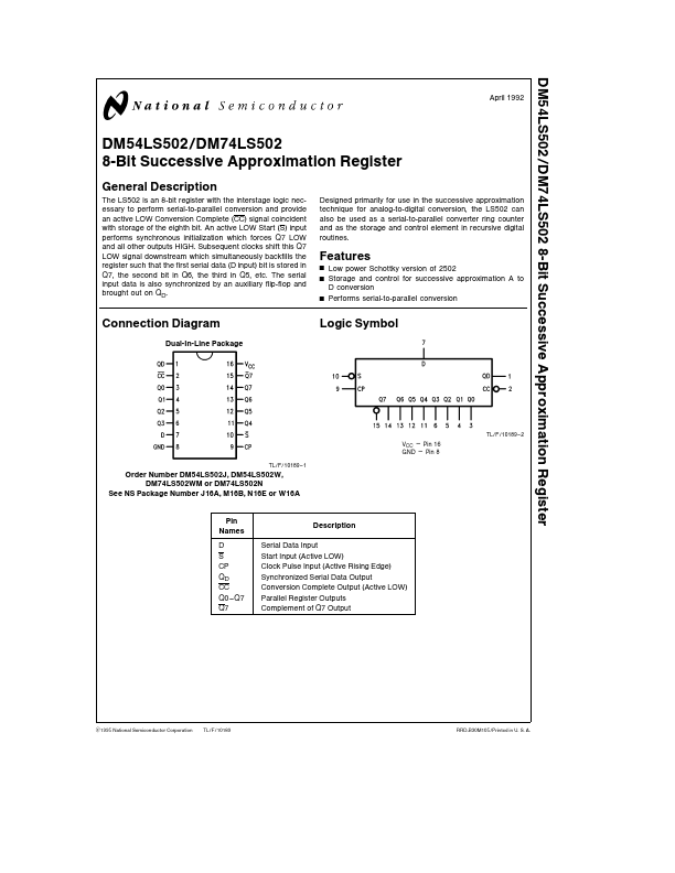
The LS502 is an 8-bit register with the interstage logic necessary to perform serial-to-parallel conversion and provide an active LOW Conversion plete (CC) signal coincident with storage of the eighth bit An active LOW Start (S) input performs synchronous initialization which forces Q7 LOW and all other outputs HIGH Subsequent clocks shift this Q7 LOW signal downstream which simultaneously backfills the register such that the first serial data (D input) bit is stored in Q7 the second bit in Q6 the third in Q5 etc The serial input data is also synchronized by an auxiliary flip-flop and brought out on QD Designed primarily for use in the successive approximation technique for analog-to-digital conversion the LS502 can also be used as a serial-to-parallel converter ring counter and as the storage and control element in recursive digital routines.