DS26S10
Description
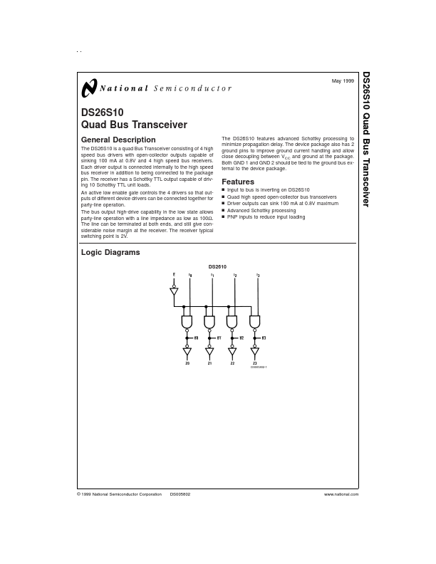
The DS26S10 is a quad Bus Transceiver consisting of 4 high speed bus drivers with open-collector outputs capable of sinking 100 mA at 0.8V and 4 high speed bus receivers.
The DS26S10 is a quad Bus Transceiver consisting of 4 high speed bus drivers with open-collector outputs capable of sinking 100 mA at 0.8V and 4 high speed bus receivers.