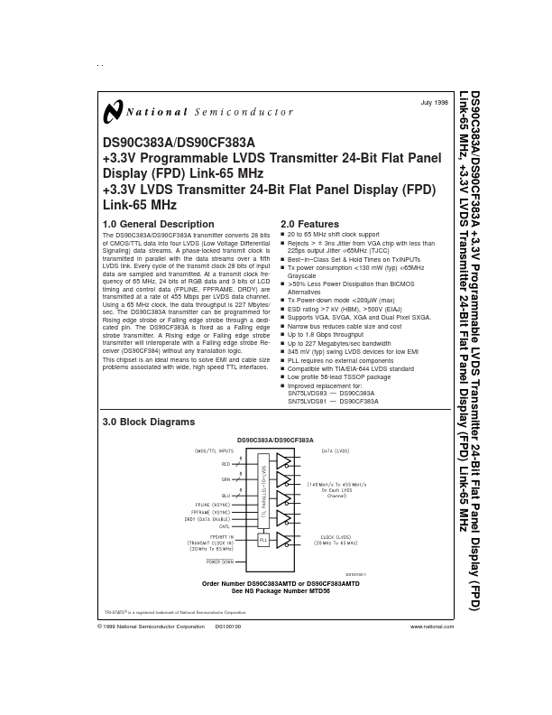
Datasheet4U Logo Datasheet4U.com

DS90C383A - +3.3V Programmable LVDS Transmitter

General Description

The DS90C383A/DS90CF383A transmitter converts 28 bits of CMOS/TTL data into four LVDS (Low Voltage Differential Signaling) data streams.

A phase-locked transmit clock is transmitted in parallel with the data streams over a fifth LVDS link.

Key Features

  • n 20 to 65 MHz shift clock support n Rejects > ± 3ns Jitter from VGA chip with less than 225ps output Jitter @65MHz (TJCC) n Best.
  • in.
  • Class Set & Hold Times on TxINPUTs n Tx power consumption < 130 mW (typ) @65MHz Grayscale n > 50% Less Power Dissipation than BiCMOS Alternatives n Tx Power-down mode < 200µW (max) n ESD rating > 7 kV (HBM), > 500V (EIAJ) n Supports VGA, SVGA, XGA and Dual Pixel SXGA. n Narrow bus reduces cable size and cost n Up to 1.8 Gbps throughput n Up to 227 M.

📥 Download Datasheet

Full PDF Text Transcription (Reference)

The following content is an automatically extracted verbatim text from the original manufacturer datasheet and is provided for reference purposes only.

View original datasheet text
DS90C383A/DS90CF383A +3.3V Programmable LVDS Transmitter 24-Bit Flat Panel Display (FPD) Link-65 MHz, +3.3V LVDS Transmitter 24-Bit Flat Panel Display (FPD) Link-65 MHz July 1998 DS90C383A/DS90CF383A +3.3V Programmable LVDS Transmitter 24-Bit Flat Panel Display (FPD) Link-65 MHz +3.3V LVDS Transmitter 24-Bit Flat Panel Display (FPD) Link-65 MHz 1.0 General Description The DS90C383A/DS90CF383A transmitter converts 28 bits of CMOS/TTL data into four LVDS (Low Voltage Differential Signaling) data streams. A phase-locked transmit clock is transmitted in parallel with the data streams over a fifth LVDS link. Every cycle of the transmit clock 28 bits of input data are sampled and transmitted.