DS90C383B Overview
Description
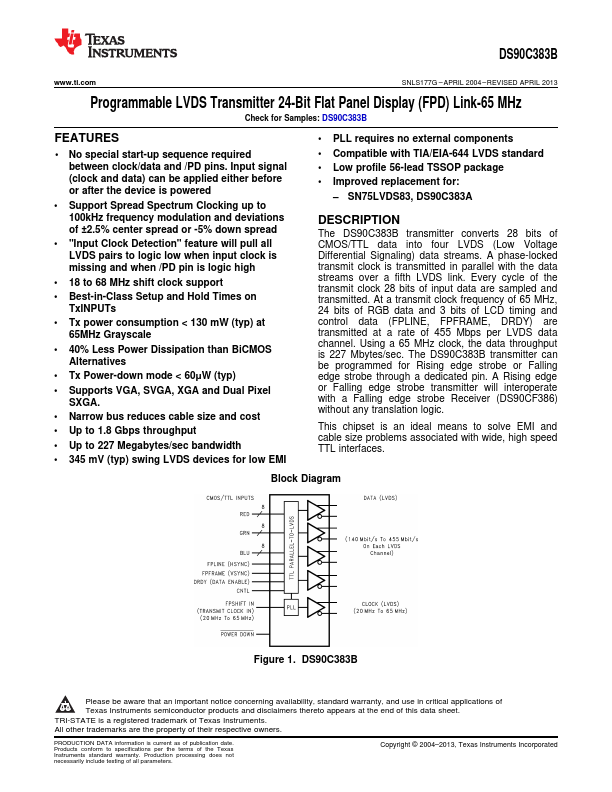
The DS90C383B transmitter converts 28 bits of CMOS/TTL data into four LVDS (Low Voltage Differential Signaling) data streams. A phase-locked transmit clock is transmitted in parallel with the data streams over a fifth LVDS link.
Key Features
- Support Spread Spectrum Clocking up to 100kHz frequency modulation and deviations of ±2.5% center spread or -5% down spread
- "Input Clock Detection" feature will pull all LVDS pairs to logic low when input clock is missing and when /PD pin is logic high
- 18 to 68 MHz shift clock support
- Best-in-Class Setup and Hold Times on TxINPUTs
- Tx power consumption < 130 mW (typ) at 65MHz Grayscale
- 40% Less Power Dissipation than BiCMOS Alternatives
- Tx Power-down mode < 60μW (typ)
- Supports VGA, SVGA, XGA and Dual Pixel SXGA
- Narrow bus reduces cable size and cost
- Up to 1.8 Gbps throughput