54F379
54F379 is Quad Parallel Register manufactured by National Semiconductor.
Description
The ’F379 is a 4-bit register with buffered mon Enable This device is similar to the ’F175 but features the mon Enable rather than mon Master Reset
Features
Y Y Y Y Y
Edge triggered D-type inputs Buffered positive edge-triggered clock Buffered mon enable input True and plement outputs Guaranteed 4000V minimum ESD protection mercial 74F379PC
Military
Package Number N16E
Package Description
16-Lead (0 300 Wide) Molded Dual-In-Line 16-Lead Ceramic Dual-In-Line 16-Lead (0 300 Wide) Molded Small Outline JEDEC 16-Lead (0 300 Wide) Molded Small Outline EIAJ 16-Lead Cerpack 20-Lead Ceramic Leadless Chip Carrier Type C
54F379DM (QB) 74F379SC (Note 1) 74F379SJ (Note 1) 54F379FM (QB) 54F379LM (QB)
J16A M16A M16D W16A E20A
Note 1 Devices also available in 13 reel Use suffix e SCX and SJX
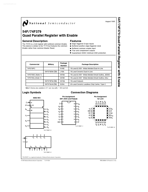
Logic Symbols
IEEE IEC
Connection Diagrams
Pin Assignment DIP SOIC and Flatpak Pin Assignment for LCC
TL F 9527
- 1 TL F 9527
- 2 TL F 9527- 5
TL F 9527- 3
TRI-STATE is a registered trademark of National Semiconductor Corporation C1995 National Semiconductor Corporation TL F 9527 RRD-B30M115 Printed in U S A
Unit Loading Fan Out
54F 74F Pin Names Description
UL Input IIH IIL HIGH LOW Output IOH IOL 10 10 10 10 10 10 50 33 3 50 33 3 20 m A b0 6 m A 20 m A b0 6 m A 20 m A b0 6 m A b 1 m A 20 m A b 1 m A 20 m A
E D 0
- D3 CP Q0
- Q3 Q0
- Q3
Enable Input (Active LOW) Data Inputs Clock Pulse Input (Active Rising Edge) Flip-Flop Outputs plement Outputs
Functional Description
The ’F379 consists of four edge-triggered D-Type flip-flops with individual D inputs and Q and Q outputs The Clock (CP) and Enable (E) inputs are mon to all flip-flops When the E is input HIGH the register will retain the present data independent of the CP input The Dn and E inputs can change when the clock is in either state provided that the remended setup and hold times are observed
Truth Table
Inputs E H L L CP L L L Dn X H L Qn NC H L Outputs Qn NC L H
H e HIGH Voltage Level L e LOW Voltage Level X e...