CD4013BM
CD4013BM is Dual D Flip-Flop manufactured by National Semiconductor.
Description
The CD4013B dual D flip-flop is a monolithic plementary MOS (CMOS) integrated circuit constructed with N- and P-channel enhancement mode transistors Each flip-flop has independent data set reset and clock inputs and ‘‘Q’’ and ‘‘Q’’ outputs These devices can be used for shift register applications and by connecting ‘‘Q’’ output to the data input for counter and toggle applications The logic level present at the ‘‘D’’ input is transferred to the Q output during the positive-going transition of the clock pulse Setting or resetting is independent of the clock and is acplished by a high level on the set or reset line respectively
Features
Wide supply voltage range High noise immunity Low power TTL patibility
3 0V to 15V 0 45 VDD (typ ) fan out of 2 driving 74L or 1 driving 74LS
Applications
Automotive Data terminals Instrumentation Medical electronics
Alarm system Industrial electronics Remote metering puters
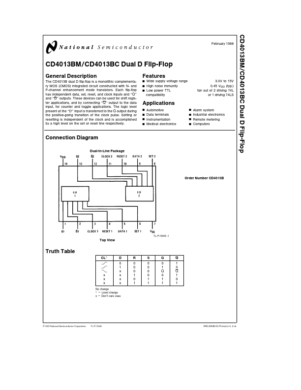
Connection Diagram
Dual-In-Line Package
Order Number CD4013B
TL F 5946
- 1
Top View
Truth Table
CL L L K x x x D 0 1 x x x x R 0 0 0 1 0 1 S 0 0 0 0 1 1 Q 0 1 Q 0 1 1 Q 1 0 Q 1 0 1
No change e Level change x e Don’t care case
C1995 National Semiconductor Corporation
TL F 5946
RRD-B30M105 Printed in U S A
Absolute Maximum Ratings (Notes 1
2)
If Military Aerospace specified devices are required please contact the National Semiconductor Sales Office Distributors for availability and specifications DC Supply Voltage (VDD) Input Voltage (VIN) Storage Temp Range (TS) Power Dissipation (PD) Dual-In-Line Small Outline Lead Temperature (TL) (Soldering 10 seconds) b 0 5 VDC to a 18 VDC b 0 5 VDC to VDD a 0 5 VDC b 65 C to a 150 C
Remended Operating Conditions (Note 2)
DC Supply Voltage (VDD) Input Voltage (VIN) Operating Temperature Range (TA) CD4013BM CD4013BC a 3 VDC to a 15 VDC
0 VDC to VDD VDC b 55 C to a 125 C b 40 C to a 85 C
700 m W 500 m W 260 C
DC Electrical Characteristics CD4013BM (Note 2)
Symbol IDD Parameter...