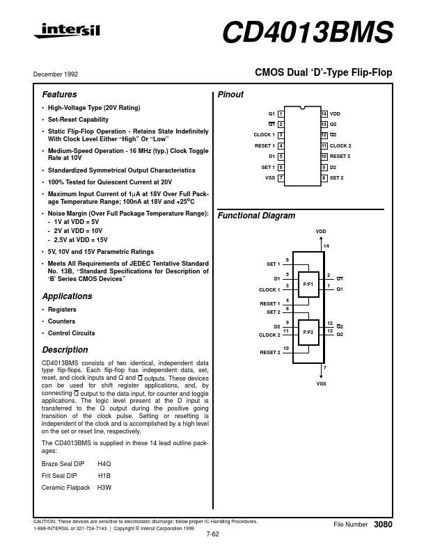
Datasheet4U Logo Datasheet4U.com

CD4013BMS - CMOS Dual D-Type Flip-Flop

Datasheet Summary

Description

of ‘B’ Series CMOS Devices” Q1 2 CLOCK 1 3 RESET 1 4 D1 5 SET 1 6 VSS 7 Functional Diagram VDD 14 6 5 3 4 8 9 11 F/F2 12 13 F/F1 2 1 SET 1 D1 CLOCK 1 Q1 Q1 Applications RESET 1 Registers Counters SET 2 D2 Q2 Q2 Control Circuits CLOCK 2 Description CD4013BMS c

Features

  • High-Voltage Type (20V Rating).
  • Set-Reset Capability.
  • Static Flip-Flop Operation - Retains State Indefinitely With Clock Level Either “High” Or “Low”.
  • Medium-Speed Operation - 16 MHz (typ. ) Clock Toggle Rate at 10V.
  • Standardized Symmetrical Output Characteristics.
  • 100% Tested for Quiescent Current at 20V.
  • Maximum Input Current of 1µA at 18V Over Full Package Temperature Range; 100nA at 18V and +25oC.
  • Noise Margin (Over Full.

📥 Download Datasheet

Datasheet preview – CD4013BMS

Datasheet Details

Part number CD4013BMS
Manufacturer Intersil Corporation
File Size 74.66 KB
Description CMOS Dual D-Type Flip-Flop
Datasheet download datasheet CD4013BMS Datasheet
Additional preview pages of the CD4013BMS datasheet.
Other Datasheets by Intersil Corporation

Full PDF Text Transcription

Click to expand full text
CD4013BMS December 1992 CMOS Dual ‘D’-Type Flip-Flop Pinout Q1 1 14 VDD 13 Q2 12 Q2 11 CLOCK 2 10 RESET 2 9 D2 8 SET 2 Features • High-Voltage Type (20V Rating) • Set-Reset Capability • Static Flip-Flop Operation - Retains State Indefinitely With Clock Level Either “High” Or “Low” • Medium-Speed Operation - 16 MHz (typ.) Clock Toggle Rate at 10V • Standardized Symmetrical Output Characteristics • 100% Tested for Quiescent Current at 20V • Maximum Input Current of 1µA at 18V Over Full Package Temperature Range; 100nA at 18V and +25oC • Noise Margin (Over Full Package Temperature Range): - 1V at VDD = 5V - 2V at VDD = 10V - 2.5V at VDD = 15V • 5V, 10V and 15V Parametric Ratings • Meets All Requirements of JEDEC Tentative Standard No.
Published: |