CD4013BM
Overview
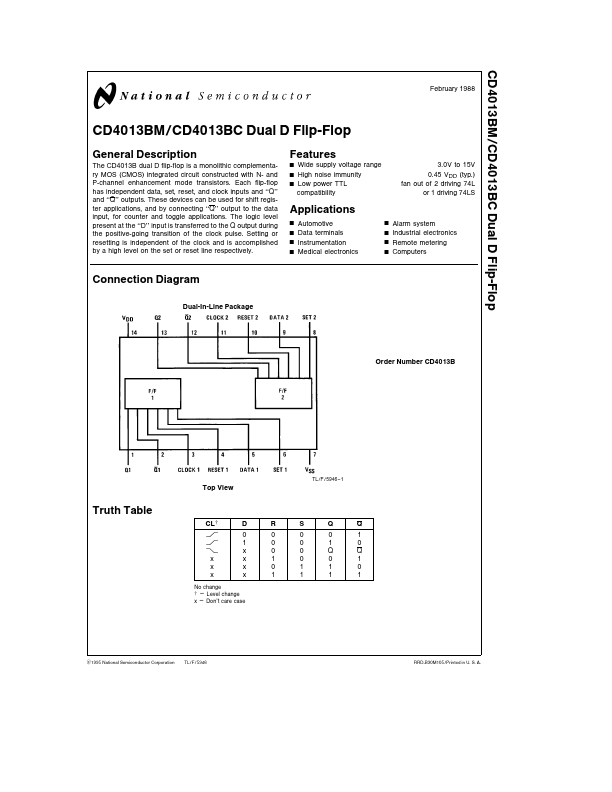
The CD4013B dual D flip-flop is a monolithic complementary MOS (CMOS) integrated circuit constructed with N- and P-channel enhancement mode transistors Each flip-flop has independent data set reset and clock inputs and ‘‘Q’’ and ‘‘Q’’ outputs These devices can be used for shift register applications and by connecting ‘‘Q’’ output to the data input for counter and toggle applications The logic level present at the ‘‘D’’ input is transferred to the Q output during the positive-going transition of the clock pulse Setting or resetting is independent of the clock and is accomplished by a high level on the set or reset line respectively.