DP84240
DP84240 is TRI-STATE Drivers Which are Designed For Heavy Capacitive Load Applications manufactured by National Semiconductor.
- Part of the DP84244 comparator family.
- Part of the DP84244 comparator family.
Description
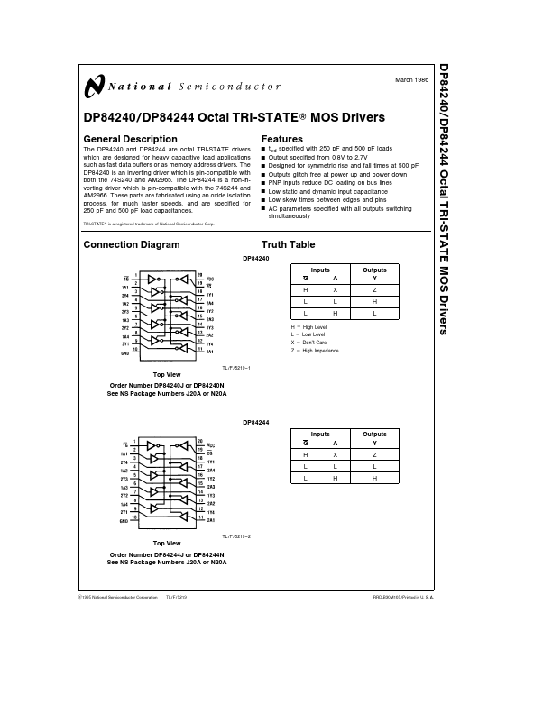
The DP84240 and DP84244 are octal TRI-STATE drivers which are designed for heavy capacitive load applications such as fast data buffers or as memory address drivers The DP84240 is an inverting driver which is pin-patible with both the 74S240 and AM2965 The DP84244 is a non-inverting driver which is pin-patible with the 74S244 and AM2966 These parts are fabricated using an oxide isolation process for much faster speeds and are specified for 250 p F and 500 p F load capacitances
TRI-STATE is a registered trademark of National Semiconductor Corp
Features
Y Y Y Y Y Y Y Y tpd specified with 250 p F and 500 p F loads Output specified from 0 8V to 2 7V Designed for symmetric rise and fall times at 500 p F Outputs glitch free at power up and power down PNP inputs reduce DC loading on bus lines Low static and dynamic input capacitance Low skew times between edges and pins AC parameters specified with all outputs switching simultaneously
Connection Diagram
Truth Table
DP84240 Inputs G H L L
H e High Level L e Low Level X e Don’t Care Z e High Impedance
TL F 5219
- 1
Outputs Y Z H L
Top View Order Number DP84240J or DP84240N See NS Package Numbers J20A or N20A
DP84244 Inputs G H L L A X L H Outputs Y Z L H
TL F 5219
- 2
Top View Order Number DP84244J or DP84244N See NS Package Numbers J20A or N20A
C1995 National Semiconductor Corporation
TL F 5219
RRD-B30M105 Printed in U S A
Absolute Maximum Ratings (Note 1)
If Military Aerospace specified devices are required please contact the National Semiconductor Sales Office Distributors for availability and specifications Supply Voltage VCC Logical ‘‘1’’ Input Voltage Logical ‘‘0’’ Input Voltage Storage Temperature Range Power Dissipation Cavity Package Molded Package Lead Temperature (soldering 10 sec ) 7 0V 7 0V b 1 5V b 65 C to a 150 C 1150 m W 1300 m W 300 C
Operating Conditions
VCC Supply Voltage TA Ambient Temperature Min 45 0 Max 55 a 70 Units V C
Electrical Characteristics VCC e 5V g 10%
Symbol...