DS26LS33M
DS26LS33M is Quad Differential Line Receivers manufactured by National Semiconductor.
Description
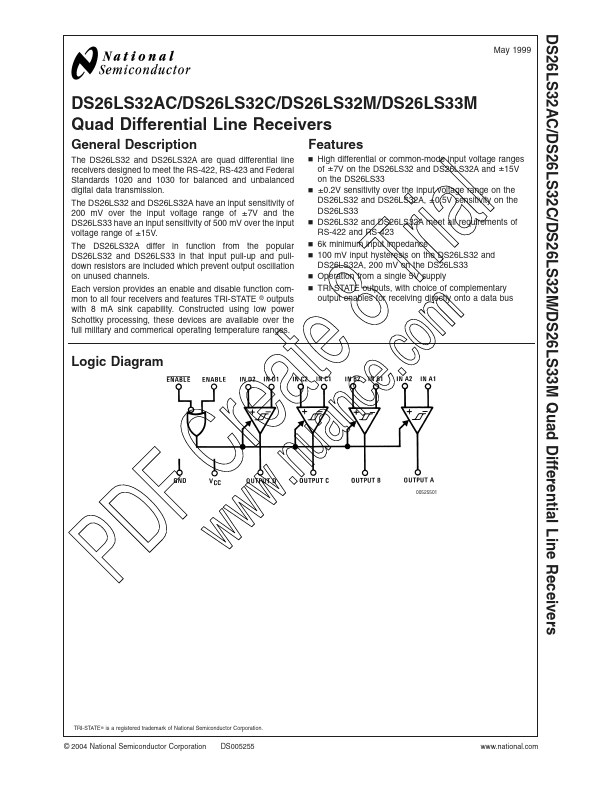
The DS26LS32 and DS26LS32A are quad differential line receivers designed to meet the RS-422, RS-423 and Federal Standards 1020 and 1030 for balanced and unbalanced digital data transmission. The DS26LS32 and DS26LS32A have an input sensitivity of 200 m V over the input voltage range of ± 7V and the DS26LS33 have an input sensitivity of 500 m V over the input voltage range of ± 15V. The DS26LS32A differ in function from the popular DS26LS32 and DS26LS33 in that input pull-up and pulldown resistors are included which prevent output oscillation on unused channels. Each version provides an enable and disable function mon to all four receivers and features
TRI-STATE ® outputs with 8 m A sink capability. Constructed using low power Schottky processing, these devices are available over the full military and merical operating temperature ranges.
Features n High differential or mon-mode input voltage ranges of ± 7V on the DS26LS32 and DS26LS32A and ± 15V on the DS26LS33 n ± 0.2V sensitivity over the input voltage range on the DS26LS32 and DS26LS32A, ± 0.5V sensitivity on the DS26LS33 n DS26LS32 and DS26LS32A meet all requirements of RS-422 and RS-423 n 6k minimum input impedance n 100 m V input hysteresis on the DS26LS32 and DS26LS32A, 200 m V on the DS26LS33 n Operation from a single 5V supply n TRI-STATE outputs, with choice of plementary output enables for receiving directly onto a data bus
Logic Diagram
F w C ww
DS005255 r e .n a ua
TRI-STATE ® is a registered trademark of National Semiconductor Corporation.
© 2004 National Semiconductor Corporation t e n ce.
.national.
8 c T om ria l http://..
DS26LS32AC/DS26LS32C/DS26LS32M/DS26LS33M
Connection Diagrams
Dual-In-Line Package 20-Lead Ceramic Leadless Chip Carrier
Truth Table
ENABLE 0 1 t e n
ENABLE Input X See
VID ≥ VTH (Max) r e .n a
Note Below
VID ≤ VTH (Min)
Hi-Z = TRI-STATE ® Note: Input conditions may be any bination not defined for ENABLE and ENABLE...