DS3245
DS3245 is Quad MOS Clock Driver manufactured by National Semiconductor.
Description
The DS3245 is a quad bipolar-to-MOS clock driver with TTL patible inputs It is designed to provide high output current and voltage capabilities necessary for optimum driving of high capacitance N-channel MOS memory systems
Only 2 supplies 5 VDC and 12 VDC are required without promising the usual high VOH specification obtained by circuits using a third supply
The device features
2 mon enable inputs a refresh input and a clock control input for simplified system designs The circuit was designed for driving highly capacitive loads at high speeds and uses Schottky-clamped transistors PNP transistors are used on all inputs thereby minimizing input loading
Features
Y TTL patible inputs Y Operates from 2 standard supplies 5 VDC 12 VDC Y Internal bootstrap circuit eliminates need for external
PNP’s Y PNP inputs minimize loading Y High voltage current outputs Y Input and output clamping diodes Y Control logic optimized for use with MOS memory sys- tems Y Pin and function equivalent to Intel 3245
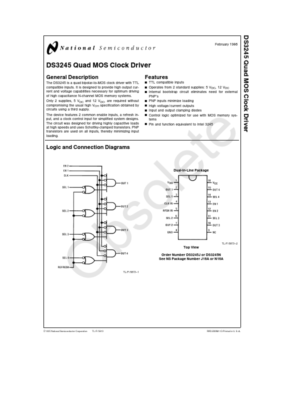
Logic and Connection Diagrams
Dual-In-Line Package
Obsolete
TL F 5873
- 1
Top View
TL F 5873
- 2
Order Number DS3245J or DS3245N See NS Package Number J16A or N16A
C1995 National Semiconductor Corporation TL F 5873
RRD-B30M115 Printed in U S A
Obsolete
Absolute Maximum Ratings
If Military Aerospace specified devices are required please contact the National Semiconductor Sales Office Distributors for availability and specifications
Temperature Under Bias b10 C to a85 C
Storage Temperature b65 C to a150 C
Supply Voltage VCC Supply Voltage VDD All Input Voltages
Outputs for Clock Driver
Maximum Power Dissipation Cavity Package Molded Package at 25 C b0 5V to a7V b0 5V to a14V b1 0V to VDD b1 0V to VDD a 1V
1509 m W 1476 m W
Derate cavity package 10 1 m W C above 25 C derate molded package 11 8 m W C above 25 C
Operating Conditions
Min Max Units
Supply Voltage VCC
4 75 5 25
Supply Voltage VDD
11 4 12 6
Operating Temperature...