Datasheet4U Logo Datasheet4U.com

JS28F128P33BF70 - 64-Mbit Single Bit per Cell Single Bit per Cell

Download the JS28F128P33BF70 datasheet PDF. This datasheet also covers the JS28F640P33TF70 variant, as both devices belong to the same 64-mbit single bit per cell single bit per cell family and are provided as variant models within a single manufacturer datasheet.

Key Features

  • Datasheet.
  • High performance:.
  • Security:.
  • 60ns initial access time for Easy BGA.
  • One-Time Programmable Registers:.
  • 70ns initial access time for TSOP.
  • 25ns 8-word asynchronous-page read mode.
  • 52MHz with zero wait states, 17ns clock-todata output synchronous-burst read mode.
  • 4-, 8-, 16-, and continuous-word options.
  • 64 OTP bits, programmed with unique information by Numonyx.
  • 2112 OTP bits, available for.

📥 Download Datasheet

Note: The manufacturer provides a single datasheet file (JS28F640P33TF70-Numonyx.pdf) that lists specifications for multiple related part numbers.

Datasheet Details

Part number JS28F128P33BF70
Manufacturer Numonyx
File Size 837.16 KB
Description 64-Mbit Single Bit per Cell Single Bit per Cell
Datasheet download datasheet JS28F128P33BF70 Datasheet

Full PDF Text Transcription (Reference)

The following content is an automatically extracted verbatim text from the original manufacturer datasheet and is provided for reference purposes only.

View original datasheet text
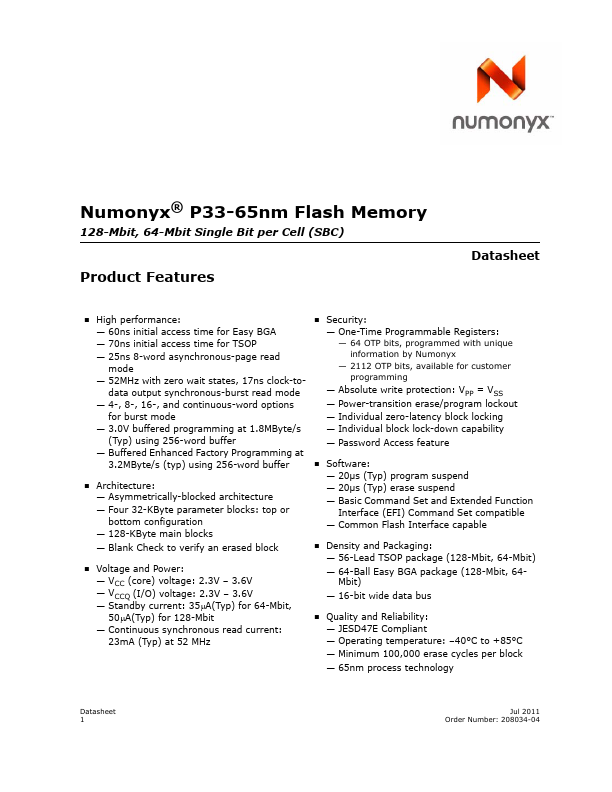
Numonyx® P33-65nm Flash Memory 128-Mbit, 64-Mbit Single Bit per Cell (SBC) Product Features Datasheet „ High performance: „ Security: — 60ns initial access time for Easy BGA — One-Time Programmable Registers: — 70ns initial access time for TSOP — 25ns 8-word asynchronous-page read mode — 52MHz with zero wait states, 17ns clock-todata output synchronous-burst read mode — 4-, 8-, 16-, and continuous-word options — 64 OTP bits, programmed with unique information by Numonyx — 2112 OTP bits, available for customer programming — Absolute write protection: VPP = VSS — Power-transition erase/program lockout for burst mode — Individual zero-latency block locking — 3.0V buffered programming at 1.