2N2222
Key Features
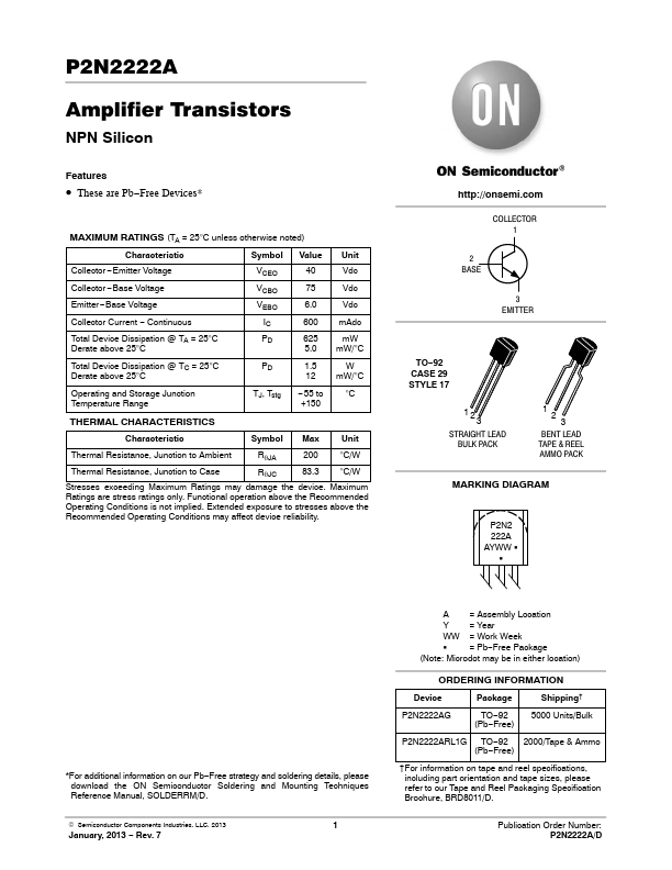
- These are Pb−Free Devices
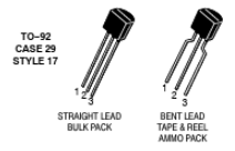
Representative 2N2222 image (package may vary by manufacturer)
Representative 2N2222 image (package may vary by manufacturer)
| Part Number | Manufacturer | Description |
|---|---|---|
| 2N2222A | SEMTECH | NPN Silicon Transistor |
| 2N2222AHR | STMicroelectronics | 50V 0.8A Hi-Rel NPN transistor |
| 2N2222AUB | Central Semiconductor | SURFACE MOUNT SILICON NPN TRANSISTOR |
| 2N2222A | Central Semiconductor | NPN SILICON TRANSISTOR |
| 2N2222 | STMicroelectronics | HIGH-SPEED SWITCHES |
| 2N2222A | MACOM Technology Solutions | Radiation Hardened NPN Silicon Switching Transistors |
| 2N2222 | Central Semiconductor | SILICON NPN TRANSISTORS |
| 2N2222 | Micro Commercial Components | NPN Switching Transistors |
| 2N2222UB | MACOM Technology Solutions | Radiation Hardened NPN Silicon Switching Transistors |
| 2N2222A | Continental Device India | NPN SILICON PLANAR SWITCHING TRANSISTORS |