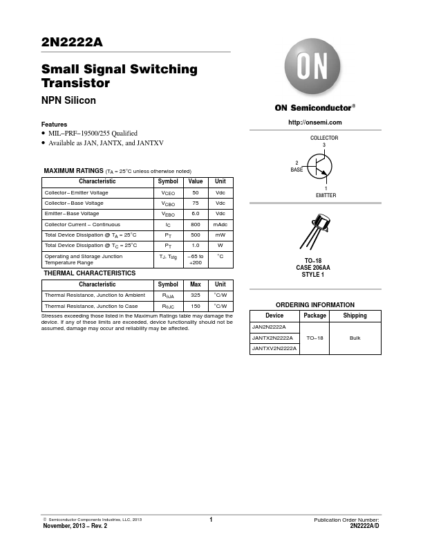
2N2222A
Key Features
- MIL-PRF-19500/255 Qualified
- Available as JAN, JANTX, and JANTXV

Representative 2N2222A image (package may vary by manufacturer)
Representative 2N2222A image (package may vary by manufacturer)
| Part Number | Manufacturer | Description |
|---|---|---|
| 2N2222A | SEMTECH | NPN Silicon Transistor |
| 2N2222AHR | STMicroelectronics | 50V 0.8A Hi-Rel NPN transistor |
| 2N2222AUB | Central Semiconductor | SURFACE MOUNT SILICON NPN TRANSISTOR |
| 2N2222A | Central Semiconductor | NPN SILICON TRANSISTOR |
| 2N2222A | MACOM Technology Solutions | Radiation Hardened NPN Silicon Switching Transistors |
| 2N2222A | Continental Device India | NPN SILICON PLANAR SWITCHING TRANSISTORS |
| 2N2222ACSM | Seme LAB | NPN SWITCHING TRANSISTOR |
| 2N2222ADCSM | Seme LAB | DUAL HIGH SPEED / MEDIUM POWER NPN SWITCHING TRANSISTOR |
| 2N2222A | Comset Semiconductor | Switching Silicon Transistors |
| 2N2222A | NTE Electronics | Silicon NPN Transistor |