Datasheet4U Logo Datasheet4U.com

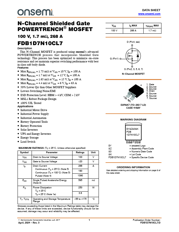
FDB1D7N10CL7 - 100V 268A N-Channel Shielded Gate MOSFET

Description

This N

Channel MOSFET is produced using onsemi’s advanced POWERTRENCH process that incorporates Shielded Gate technology.

state resistance and yet maintain superior switching performance with best in class soft body diode.

Features

  • Max RDS(on) = 1.75 mΩ at VGS = 10 V, ID = 100 A.
  • Max RDS(on) = 1.7 mΩ at VGS = 12 V, ID = 100 A.
  • Max RDS(on) = 1.65 mΩ at VGS = 15 V, ID = 100 A.
  • Max RDS(on) = 4.4 mΩ at VGS = 6 V, ID = 63 A.
  • 50% Lower Qrr than Other MOSFET Suppliers.
  • Lowers Switching Noise/EMI.
  • ESD Protection Level: HBM > 4 kV, CDM > 2 kV.
  • MSL1 Robust Package Design.
  • 100% UIL Tested.

📥 Download Datasheet

Datasheet preview – FDB1D7N10CL7

Datasheet Details

Part number FDB1D7N10CL7
Manufacturer ON Semiconductor
File Size 349.38 KB
Description 100V 268A N-Channel Shielded Gate MOSFET
Datasheet download datasheet FDB1D7N10CL7 Datasheet
Additional preview pages of the FDB1D7N10CL7 datasheet.
Other Datasheets by ON Semiconductor

Full PDF Text Transcription

Click to expand full text
N-Channel Shielded Gate POWERTRENCH) MOSFET 100 V, 1.7 mW, 268 A FDB1D7N10CL7 Description This N−Channel MOSFET is produced using onsemi’s advanced POWERTRENCH process that incorporates Shielded Gate technology. This process has been optimized to minimize on−state resistance and yet maintain superior switching performance with best in class soft body diode. Features • Max RDS(on) = 1.75 mΩ at VGS = 10 V, ID = 100 A • Max RDS(on) = 1.7 mΩ at VGS = 12 V, ID = 100 A • Max RDS(on) = 1.65 mΩ at VGS = 15 V, ID = 100 A • Max RDS(on) = 4.
Published: |