FDC6323L
Description
These Integrated Load Switches are produced using onsemi’s proprietary, high cell density, DMOS technology. This very high density process is especially tailored to minimize on- state resistance and provide superior switching performance. These devices are particularly suited for low voltage high side load switch application where low conduction loss and ease of driving are needed.
Features
- VDROP = 0.2 V @ VIN = 5 V, IL = 1 A, VON/OFF = 1.5 V to 8 V
- VDROP = 0.3 V @ VIN = 3.3 V, IL = 1 A, VON/OFF = 1.5 V to 8 V
- High Density Cell Design for Extremely Low On- Resistance
- VON/OFF Zener Protection for ESD Ruggedness > 6 k V Human
Body Model
- SUPERSOTt- 6 Package Design Using Copper Lead Frame for
Superior Thermal and Electrical Capabilities
- This is a Pb- Free and Halide Free Device
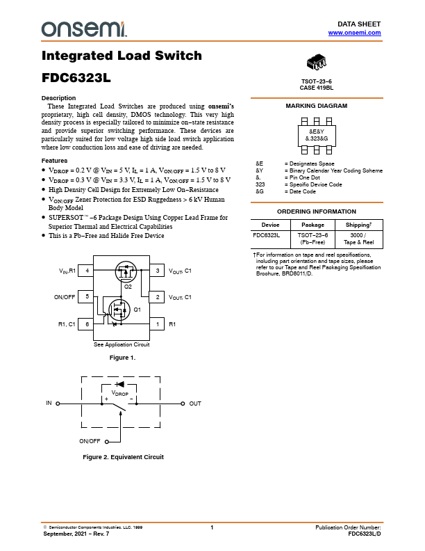
VIN,R1 4 ON/OFF 5
R1, C1 6
Q2 Q1
3 VOUT, C1 2 VOUT, C1 1 R1
See Application Circuit Figure 1.
DATA SHEET .onsemi.
TSOT- 23- 6 CASE 419BL
MARKING DIAGRAM
&E&Y &.323&G
&E
= Designates...