FDC6325L
Description
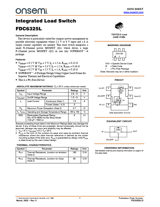
This device is particularly suited for pact power management in portable electronic equipment where 2.5 V to 8 V input and 1.8 A output current capability are needed. This load switch integrates a small N- Channel power MOSFET (Q1) which drives a large P- Channel power MOSFET (Q2) in one tiny SUPERSOTt- 6 package.
Features
- VDROP = 0.2 V @ VIN = 5 V, IL = 1.5 A, R(ON) = 0.13 W
VDROP = 0.2 V @ VIN = 3.3 V, IL = 1.2 A, R(ON) = 0.16 W VDROP = 0.2 V @ VIN = 2.5 V, IL = 1 A, R(ON) = 0.18 W
- SUPERSOTt- 6 Package Design Using Copper Lead Frame for
Superior Thermal and Electrical Capabilities
- This is a Pb- Free Device
ABSOLUTE MAXIMUM RATINGS (TA = 25°C unless otherwise noted)
Symbol
Parameter
Ratings Unit
VIN Input Voltage Range
- 8
VON/OFF On/Off Voltage Range
- 8
Load Current
Continuous (Note 1)
Pulsed (Notes 1 & 3)
Maximum Power Dissipation (Note 2)
TJ, TSTG Operating and Storage Temperature Range
- 55 to 150...