FDC6329L
Description
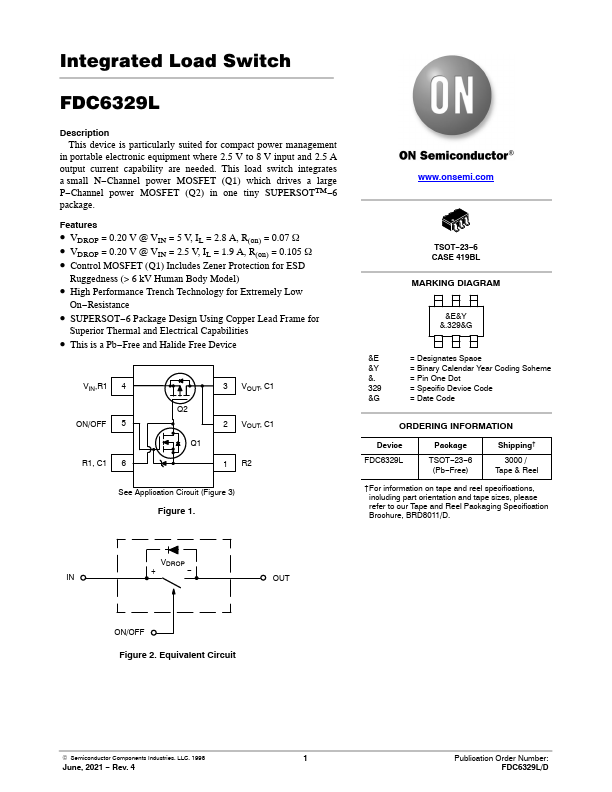
This device is particularly suited for pact power management in portable electronic equipment where 2.5 V to 8 V input and 2.5 A output current capability are needed. This load switch integrates a small N- Channel power MOSFET (Q1) which drives a large P- Channel power MOSFET (Q2) in one tiny SUPERSOTTM- 6 package.
Features
- VDROP = 0.20 V @ VIN = 5 V, IL = 2.8 A, R(on) = 0.07 W
- VDROP = 0.20 V @ VIN = 2.5 V, IL = 1.9 A, R(on) = 0.105 W
- Control MOSFET (Q1) Includes Zener Protection for ESD
Ruggedness (> 6 k V Human Body Model)
- High Performance Trench Technology for Extremely Low
On- Resistance
- SUPERSOT- 6 Package Design Using Copper Lead Frame for
Superior Thermal and Electrical Capabilities
- This is a Pb- Free and Halide Free Device
VIN,R1 4 ON/OFF 5
R1, C1 6
Q2 Q1
3 VOUT, C1 2 VOUT, C1 1 R2
See Application Circuit (Figure 3) Figure 1.
.onsemi.
TSOT- 23- 6 CASE 419BL
MARKING DIAGRAM
&E&Y &.329&G
&E
= Designates Space
&Y
= Binary Calendar Year Coding...