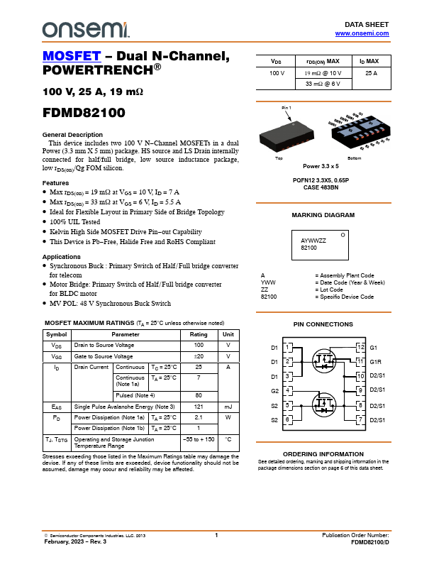
FDMD82100
Overview
This device includes two 100 V N-Channel MOSFETs in a dual Power (3.3 mm X 5 mm) package. HS source and LS Drain internally connected for half/full bridge, low source inductance package, low rDS(on)/Qg FOM silicon.
- Max rDS(on) = 19 mW at VGS = 10 V, ID = 7 A
- Max rDS(on) = 33 mW at VGS = 6 V, ID = 5.5 A
- Ideal for Flexible Layout in Primary Side of Bridge Topology
- 100% UIL Tested
- Kelvin High Side MOSFET Drive Pin-out Capability
- This Device is Pb-Free, Halide Free and RoHS Compliant