FDME910PZT-P
Description
This device is designed specifically for battery charging or load switching in cellular handset and other ultraportable applications. It features a MOSFET with low on-state resistance and zener diode protection against ESD.
Key Features
- Max RDS(on) = 24 mW at VGS = -4.5 V, ID = -8 A
- Max RDS(on) = 31 mW at VGS = -2.5 V, ID = -7 A
- Max RDS(on) = 45 mW at VGS = -1.8 V, ID = -6 A
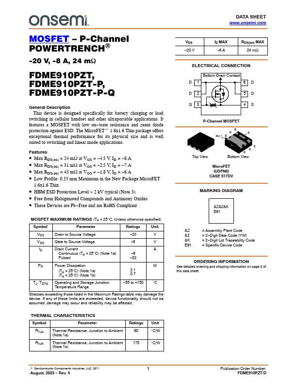
- Low Profile: 0.55 mm Maximum in the New Package MicroFET 1.6x1.6 Thin
- HBM ESD Protection Level > 2 kV typical (Note
- Free from Halogenated pounds and Antimony Oxides
- These Devices are Pb-Free and are RoHS compliant MOSFET Symbol Parameter Ratings Unit VDS Drain to Source Voltage
- 20 V VGS Gate to Source Voltage ±8 V ID Drain Current A Continuous (TA = 25°C) (Note 1a)
- 32 PD TJ, TSTG Power Dissipation (TA = 25°C) (Note 1a) (TA = 25°C) (Note 1b) Operating and Storage Junction Temperature Range W 2.1 0.7