FIN1001 Overview
Key Specifications
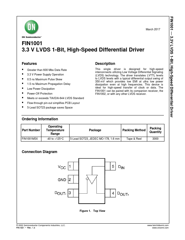
Package: LSSOP
Mount Type: Surface Mount
Pins: 5
Operating Voltage: 3.3 V
Description
This single driver is designed for high-speed interconnects utilizing Low Voltage Differential Signaling (LVDS) technology. The driver translates LVTTL levels to LVDS levels with a typical differential output swing of 350 mV which provides low EMI at ultra low power dissipation even at high frequencies.
Key Features
- Greater than 600 Mbs Data Rate
- 3.3 V Power Supply Operation
- 0.5 ns Maximum Pulse Skew
- 1.5 ns Maximum Propagation Delay
- Low Power Dissipation