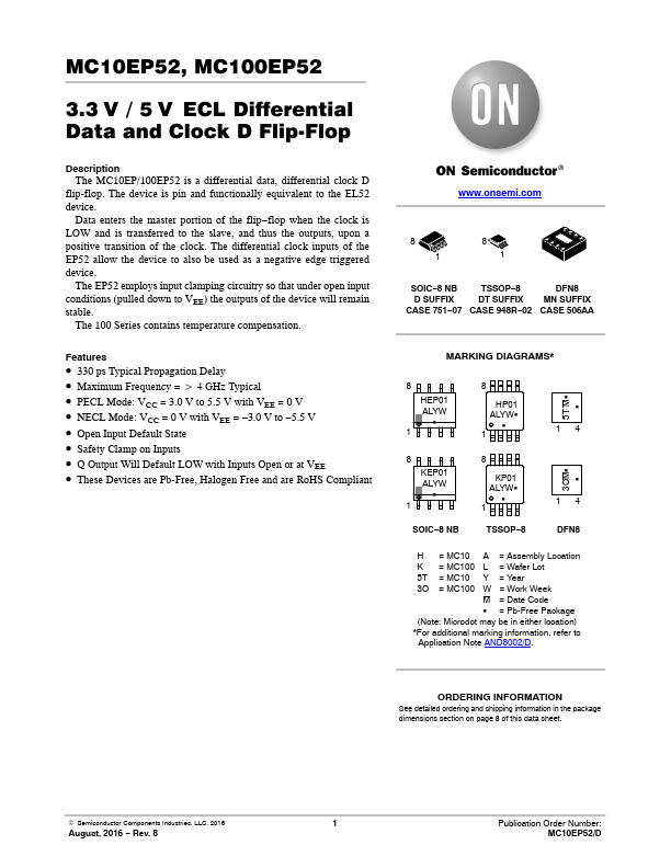
MC100EP52 Description
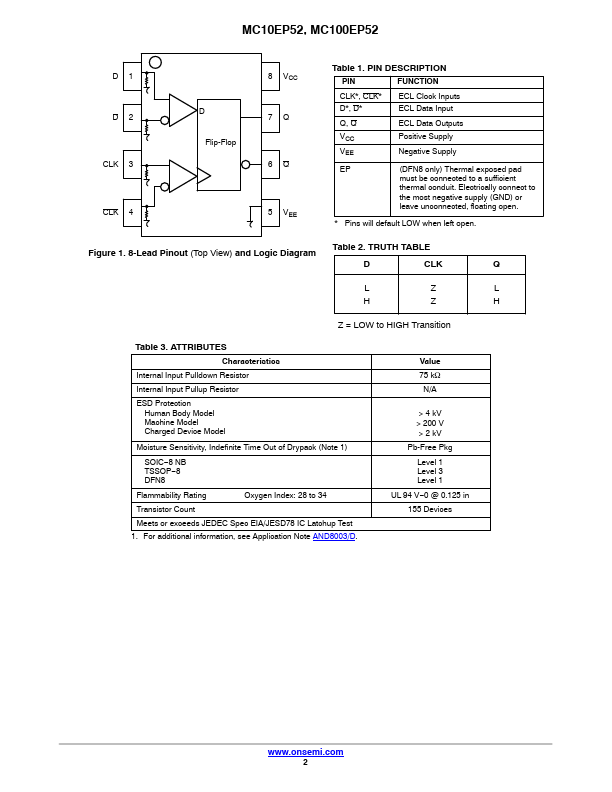
The MC10EP/100EP52 is a differential data, differential clock D flip-flop. The device is pin and functionally equivalent to the EL52 device. Data enters the master portion of the flip−flop when the clock is LOW and is transferred to the slave, and thus the outputs, upon a positive transition of the clock.
MC100EP52 Key Features
- 330 ps Typical Propagation Delay
- Maximum Frequency = u 4 GHz Typical
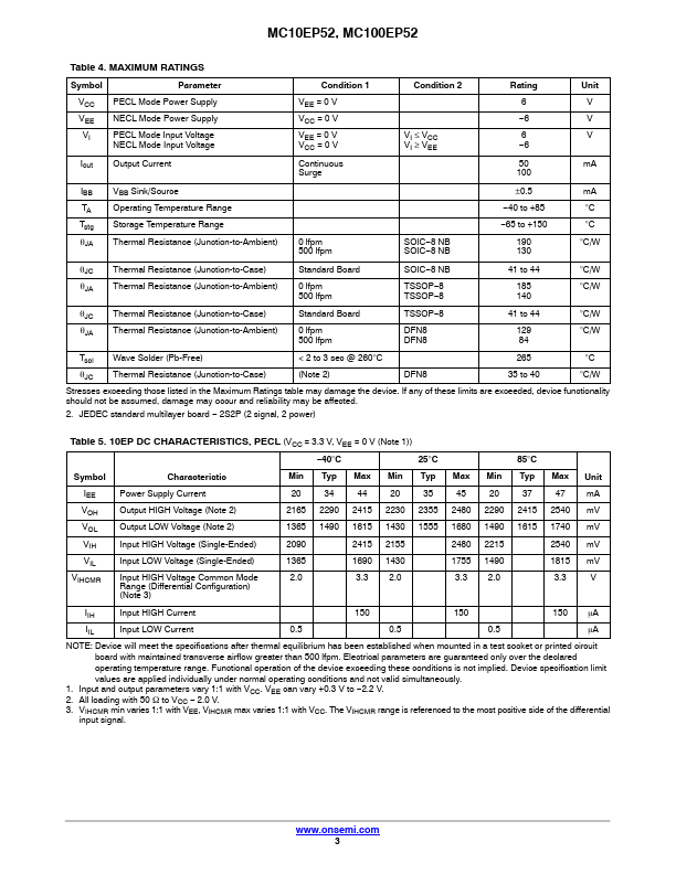
- PECL Mode: VCC = 3.0 V to 5.5 V with VEE = 0 V
- NECL Mode: VCC = 0 V with VEE = -3.0 V to -5.5 V
- Open Input Default State
- Safety Clamp on Inputs
- Q Output Will Default LOW with Inp