MC100LVEL39 Overview
Key Specifications
Package: SOP
Mount Type: Surface Mount
Pins: 20
Operating Voltage: 3.3 V
Description
The MC100LVEL39 is a low skew ÷2/4, ÷4/6 clock generation chip designed explicitly for low skew clock generation applications. The internal dividers are synchronous to each other, therefore, the common output edges are all precisely aligned.
Key Features
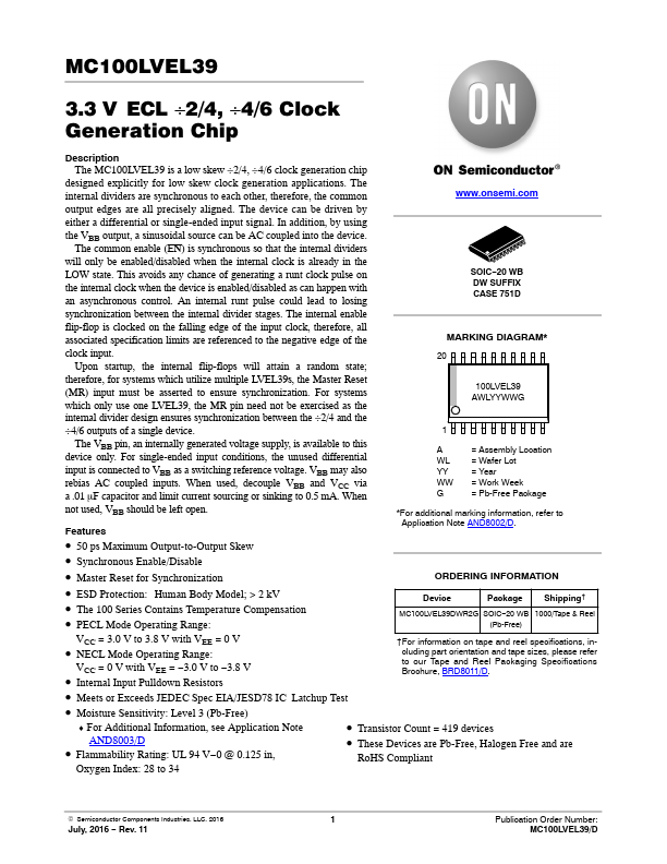
- SOIC-20 WB DW SUFFIX CASE 751D MARKING DIAGRAM* 20 100LVEL39 AWLYYWWG 1 A = Assembly Location WL = Wafer Lot YY = Year WW