MPSA18
MPSA18 is Low Noise Transistor manufactured by onsemi.
Features
- These are Pb- Free Devices-
MAXIMUM RATINGS
Rating Collector
- Emitter Voltage Collector
- Base Voltage Emitter
- Base Voltage Collector Current
- Continuous Total Device Dissipation @ TA = 25°C Derate above 25°C
Symbol VCEO VCBO VEBO
IC PD
Value 45 45 6.5 200 625 5.0
Unit Vdc Vdc Vdc m Adc m W m W/°C
Total Device Dissipation @ TC = 25°C
Derate above 25°C
12 m W/°C
Operating and Storage Junction Temperature Range
TJ, Tstg
- 55 to +150 °C
THERMAL CHARACTERISTICS
Characteristic
Symbol
Max
Thermal Resistance, Junction- to- Ambient Rq JA
(Note 1)
Unit °C/W
Thermal Resistance, Junction- to- Case
Rq JC
°C/W
Maximum ratings are those values beyond which device damage can occur. Maximum ratings applied to the device are individual stress limit values (not normal operating conditions) and are not valid simultaneously. If these limits are exceeded, device functional operation is not implied, damage may occur and reliability may be affected. 1. RθJA is measured with the device soldered into a typical printed circuit board.
- For additional information on our Pb- Free strategy and soldering details, please download the ON Semiconductor Soldering and Mounting Techniques Reference Manual, SOLDERRM/D.
© Semiconductor ponents Industries, LLC, 2007
April, 2007
- Rev. 4 http://onsemi.
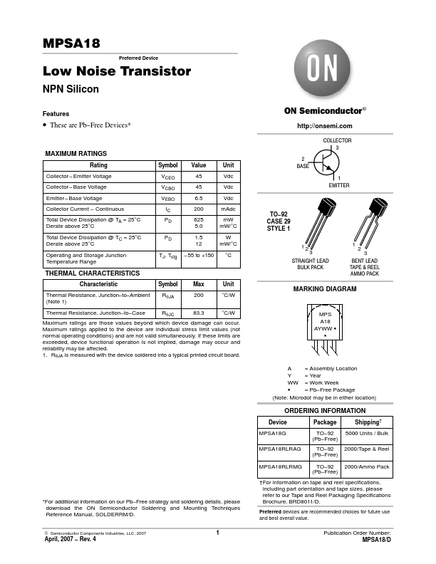
2 BASE
COLLECTOR 3
1...