MTD10N10EL
MTD10N10EL is Power Field Effect Transistor DPAK manufactured by onsemi.
MTD10N10EL TMOS E- FET™ Power Field Effect Transistor DPAK for Surface Mount
N- Channel Enhancement- Mode Silicon Gate
This advanced TMOS E- FET is designed to withstand high energy in the avalanche and mutation modes. The new energy efficient design also offers a drain- to- source diode with a fast recovery time. Designed for low voltage, high speed switching applications in power supplies, converters and PWM motor controls, these devices are particularly well suited for bridge circuits where diode speed and mutating safe operating areas are critical and offer additional safety margin against unexpected voltage transients.
Features
VDSS 100 V http://onsemi.
RDS(ON) TYP 0.22 W
ID MAX 10 A
N- Channel D
- Avalanche Energy Specified
- Source- to- Drain Diode Recovery Time parable to a Discrete
- -
- Fast Recovery Diode Diode is Characterized for Use in Bridge Circuits IDSS and VDS(on) Specified at Elevated Temperature Pb- Free Package is Available
MAXIMUM RATINGS (TC = 25°C unless otherwise noted) ..
Parameter Drain- to- Source Voltage Drain- to- Gate Voltage (RGS = 1.0 MW) Gate- to- Source Voltage
- Continuous Non- Repetitive (tp ≤ 10 ms) Drain Current
- Continuous
- Continuous @ 100°C
- Single Pulse (tp ≤ 10 ms) Symbol VDSS VDGR VGS VGSM ID ID IDM PD Value 100 100 ±15 ±20 10 6.0 35 40 0.32 1.75
- 55 to 150 50 Unit Vdc Vdc Vdc Vpk Adc Apk W W/°C W °C m J
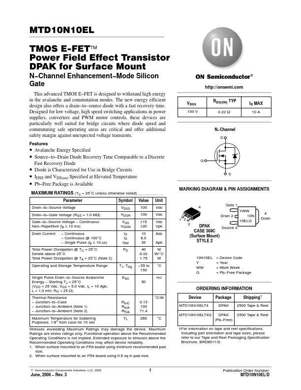
MARKING DIAGRAM & PIN ASSIGNMENTS
4 1 2 3
Gate 1 Drain 2 YWW 10N 10ELG 4 Drain
DPAK Source 3 CASE 369C (Surface Mount) STYLE 2
Total Power Dissipation @ TC = 25°C Derate above 25°C Total Power Dissipation @ TA = 25°C (Note 2) Operating and Storage Temperature Range Single Pulse Drain- to- Source Avalanche Energy
- Starting TJ = 25°C (VDD = 25 Vdc, VGS = 5.0 Vdc, IL = 10 Apk, L = 1.0 m H, RG = 25 W) Thermal Resistance
- Junction- to- Case
- Junction- to- Ambient (Note 1)
- Junction- to- Ambient (Note 2) Maximum Temperature for Soldering Purposes, 1/8″ from case for 10 sec
TJ, Tstg EAS
10N10EL Y WW...