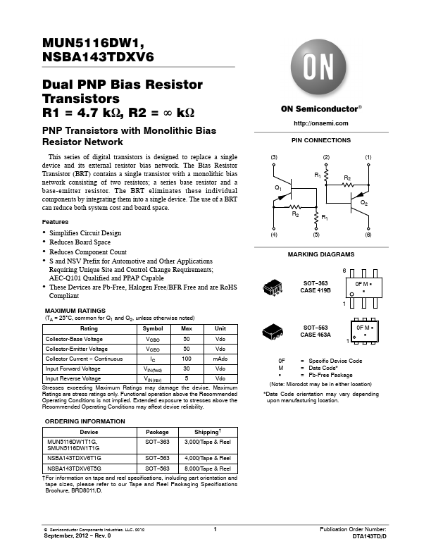
MUN5116DW1
Features
- Simplifies Circuit Design
- Reduces Board Space
- Reduces ponent Count
- S and NSV Prefix for Automotive and Other Applications
Requiring Unique Site and Control Change Requirements; AEC-Q101 Qualified and PPAP Capable
- These Devices are Pb-Free, Halogen Free/BFR Free and are Ro HS pliant
MAXIMUM RATINGS (TA = 25C, mon for Q1 and Q2, unless otherwise noted)
Rating
Symbol
Max
Unit
Collector-Base Voltage
VCBO
Vdc
Collector-Emitter Voltage
VCEO
Vdc
Collector Current
- Continuous IC 100 m Adc
Input Forward Voltage
VIN(fwd)
Vdc
Input Reverse Voltage
VIN(rev)
Vdc
Stresses exceeding Maximum Ratings may damage the device. Maximum Ratings are stress ratings only. Functional operation above the Remended Operating Conditions is not implied. Extended exposure to stresses above the Remended Operating Conditions may affect device reliability.
ORDERING INFORMATION
Device
Package
Shipping†
MUN5116DW1T1G, SMUN5116DW1T1G
SOT- 363
3,000/Tape &...