MUN5116DW1T1
Features http://onsemi.
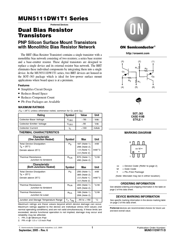
(3) R1 Q1 Q2 R2 (4) R1 (5) (6) (2) R2 (1)
- -
- -
Simplifies Circuit Design Reduces Board Space Reduces ponent Count Pb- Free Packages are Available
MAXIMUM RATINGS
(TA = 25°C unless otherwise noted, mon for Q1 and Q2) Rating Collector-Base Voltage Collector-Emitter Voltage Collector Current Symbol VCBO VCEO IC Value Unit SOT- 363 CASE 419B STYLE 1
..
- 50 Vdc
- 50
- 100
Vdc m Adc
THERMAL CHARACTERISTICS
Characteristic (One Junction Heated) Total Device Dissipation TA = 25°C Derate above 25°C Thermal Resistance, Junction-to-Ambient Characteristic (Both Junctions Heated) Total Device Dissipation TA = 25°C Derate above 25°C Thermal Resistance, Junction-to-Ambient Thermal Resistance, Junction-to-Lead Junction and Storage Temperature Range Symbol PD Max 187 (Note 1) 256 (Note 2) 1.5 (Note 1) 2.0 (Note 2) 670 (Note 1) 490 (Note 2) Max 250 (Note 1) 385 (Note 2) 2.0 (Note 1) 3.0 (Note 2) 493 (Note 1) 325 (Note 2) 188 (Note 1) 208 (Note 2)
- 55 to +150 Unit m W m W/°C...