Datasheet Summary
2.5 V/3.3 V Quad Differential Driver/Receiver
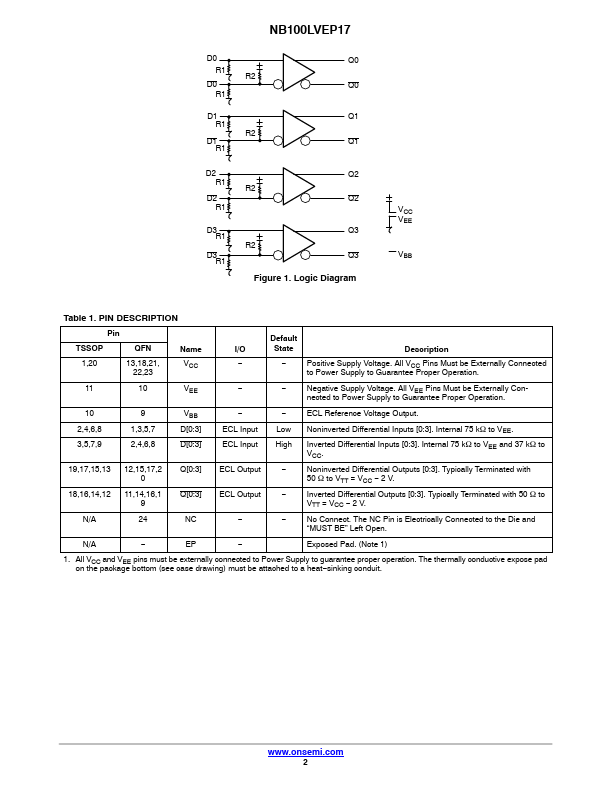
Description The NB100LVEP17 is a 4-bit differential line receiver. The design incorporates two stages of gain, internal to the device, making it an excellent choice for use in high bandwidth amplifier applications.
The VBB pin, an internally generated voltage supply, is available to this device only. For single-ended input conditions, the unused differential input is connected to VBB as a switching reference voltage. VBB may also rebias AC coupled inputs. When used, decouple VBB and VCC via a 0.01 mF capacitor and limit current sourcing or sinking to 0.5 mA. When not used, VBB should be left open.
Inputs of unused gates can be left...