NB2304A
NB2304A is Zero Delay Clock Buffer manufactured by onsemi.
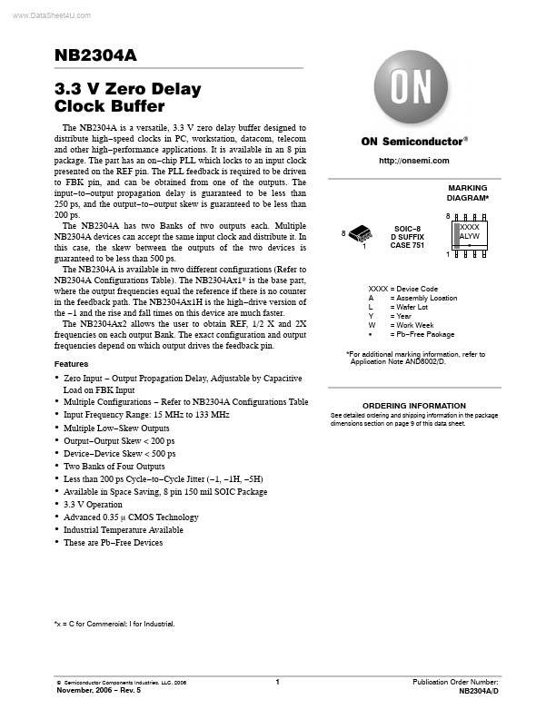
Features http://onsemi. MARKING DIAGRAM-
8 8 1 SOIC- 8 D SUFFIX CASE 751 1 XXXX ALYW G
XXXX A L Y W G
= Device Code = Assembly Location = Wafer Lot = Year = Work Week = Pb- Free Package
- For additional marking information, refer to Application Note AND8002/D.
- Zero Input
- Output Propagation Delay, Adjustable by Capacitive
- -
- -
- -
- -
- -
- -
Load on FBK Input Multiple Configurations
- Refer to NB2304A Configurations Table Input Frequency Range: 15 MHz to 133 MHz Multiple Low- Skew Outputs Output- Output Skew < 200 ps Device- Device Skew < 500 ps Two Banks of Four Outputs Less than 200 ps Cycle- to- Cycle Jitter (- 1,
- 1H,
- 5H) Available in Space Saving, 8 pin 150 mil SOIC Package 3.3 V Operation Advanced 0.35 m CMOS Technology Industrial Temperature Available These are Pb- Free Devices
ORDERING INFORMATION
See detailed ordering and shipping information in the package dimensions section on page 9 of this data sheet.
- x = C for mercial; I for Industrial.
© Semiconductor ponents Industries, LLC, 2006
November, 2006
- Rev. 5
Publication Order Number: NB2304A/D
CLKA1 REF PLL CLKA2
B2
Extra Divider (- 2) CLKB1
CLKB2
Figure 1. Basic Block Diagram (see Figures 11 and 12 for device specific Block Diagrams)
Table 1. CONFIGURATIONS (x = C for mercial; I for Industrial)
Device NB2304Ax1 NB2304Ax1H NB2304Ax2 NB2304Ax2 Feedback From Bank A or Bank B Bank A or Bank B Bank A Bank B Bank A Frequency Reference Reference Reference 2 X Reference Bank B Frequency Reference Reference Reference B2 Reference
REF CLKA1 CLKA2 GND
1 2
8 7
FBK VDD CLKB2 CLKB1
Table 2. PIN DESCRIPTION
Pin # 1 2 3 4 5 Pin Name REF...