NB2305A
NB2305A is Zero Delay Clock Buffer manufactured by onsemi.
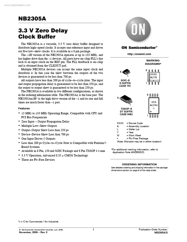
Features http://onsemi. MARKING DIAGRAMS-
8 1 SOIC- 8 D SUFFIX CASE 751 1 8 XXXX ALYW G
8 8 1 TSSOP- 8 DT SUFFIX CASE 948J XXX ALYWG G 1
- 15 MHz to 133 MHz Operating Range, patible with CPU and
- -
- -
- -
- -
- PCI Bus Frequencies Zero Input
- Output Propagation Delay Multiple Low- Skew Outputs Output- Output Skew Less than 250 ps Device- Device Skew Less than 700 ps One Input Drives 5 Outputs Less than 200 ps Cycle- to- Cycle Jitter is patible with Pentium R Based Systems Available in 8 Pin, 150 mil SOIC Package and 8 Pin TSSOP 4.4 mm 3.3 V Operation, Advanced 0.35 m CMOS Technology These are Pb- Free Devices
XXXX = Device Code A = Assembly Location L = Wafer Lot Y = Year W = Work Week G = Pb- Free Package (Note: Microdot may be in either location)
- For additional marking information, refer to Application Note AND8002/D.
ORDERING INFORMATION
See detailed ordering and shipping information in the package dimensions section on page 6 of this data sheet.
- x = C for mercial; I for Industrial.
© Semiconductor ponents Industries, LLC, 2006
November, 2006
- Rev. 5
Publication Order Number: NB2305A/D
CLKOUT REF CLK2 CLK2 CLK1 CLK3 GND 3 4 1 2 8 7 CLKOUT CLK4 VDD CLK3
CLK1
6 5
CLK4
Figure 1. Block Diagram
Figure 2. Pin Configuration
Table 1. PIN DESCRIPTION
Pin # Pin Name Description
1 2 3 4 5 6 7 8
REF (Note1) CLK2 (Note 2) CLK1 (Note 2) GND CLK3 (Note 2) VDD CLK4 (Note 2) CLKOUT (Note 2)
Input reference frequency, 5 V tolerant input. Buffered clock output. Buffered clock output. Ground. Buffered clock output. 3.3 V supply. Buffered clock output. Buffered clock output, internal feedback on this pin.
1. Weak pulldown. 2. Weak pulldown on all outputs. http://onsemi.
Table 2. MAXIMUM RATINGS
Parameter Supply Voltage to Ground Potential DC Input Voltage (Except REF) DC Input Voltage (REF)...