NB2309A
NB2309A is 3.3 V Zero Delay Clock Buffer manufactured by onsemi.
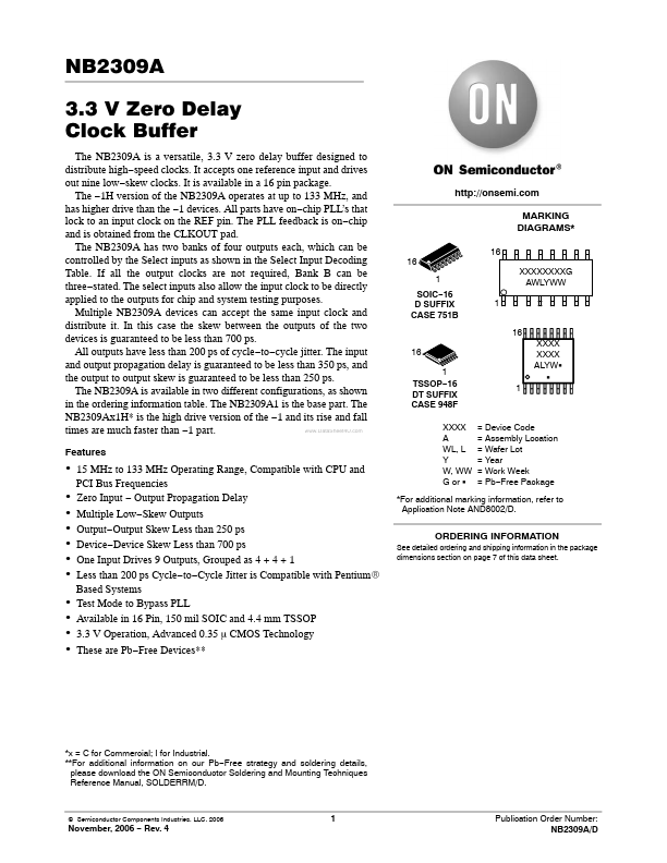
Features http://onsemi. MARKING DIAGRAMS-
16 1 SOIC- 16 D SUFFIX CASE 751B 1 16 16 1 TSSOP- 16 DT SUFFIX CASE 948F XXXX A WL, L Y W, WW G or G XXXX XXXX ALYWG G 16 XXXXXXXXG AWLYWW
- 15 MHz to 133 MHz Operating Range, patible with CPU and
- -
- -
- -
- -
- -
PCI Bus Frequencies Zero Input
- Output Propagation Delay Multiple Low- Skew Outputs Output- Output Skew Less than 250 ps Device- Device Skew Less than 700 ps One Input Drives 9 Outputs, Grouped as 4 + 4 + 1 Less than 200 ps Cycle- to- Cycle Jitter is patible with Pentium R Based Systems Test Mode to Bypass PLL Available in 16 Pin, 150 mil SOIC and 4.4 mm TSSOP 3.3 V Operation, Advanced 0.35 m CMOS Technology These are Pb- Free Devices-
- = Device Code = Assembly Location = Wafer Lot = Year = Work Week = Pb- Free Package
- For additional marking information, refer to Application Note AND8002/D.
ORDERING INFORMATION
See detailed ordering and shipping information in the package dimensions section on page 7 of this data sheet.
- x = C for mercial; I for Industrial.
- - For additional information on our Pb- Free strategy and soldering details, please download the ON Semiconductor Soldering and Mounting Techniques Reference Manual, SOLDERRM/D.
© Semiconductor ponents Industries, LLC, 2006
November, 2006
- Rev. 4
Publication Order Number: NB2309A/D
PLL REF
CLKOUT
CLKA1
CLKA2
CLKA3
S2 SELECT INPUT DECODING S1
CLKA4
CLKB1
CLKB2
CLKB3
CLKB4
Figure 1. Block Diagram
Table 1. SELECT INPUT DECODING
S2 0 0 1 1 S1 0 1 0 1 Clock A1
- A4 Three-...