NB2769A
NB2769A is Reduced EMI Clock Synthesizer manufactured by onsemi.
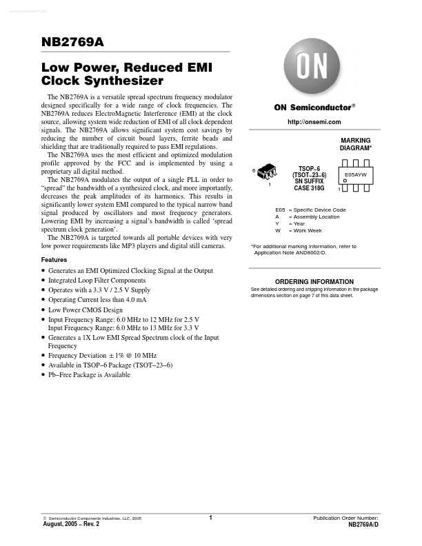
Features http://onsemi. MARKING DIAGRAM-
TSOP- 6 (TSOT- 23- 6) SN SUFFIX CASE 318G
6 1
E05AYW 1
E05 A Y W
= Specific Device Code = Assembly Location = Year = Work Week
- For additional marking information, refer to Application Note AND8002/D.
- -
- -
- -
- -
- -
Generates an EMI Optimized Clocking Signal at the Output Integrated Loop Filter ponents Operates with a 3.3 V / 2.5 V Supply Operating Current less than 4.0 m A Low Power CMOS Design Input Frequency Range: 6.0 MHz to 12 MHz for 2.5 V Input Frequency Range: 6.0 MHz to 13 MHz for 3.3 V Generates a 1X Low EMI Spread Spectrum clock of the Input Frequency Frequency Deviation "1% @ 10 MHz Available in TSOP- 6 Package (TSOT- 23- 6) Pb- Free Package is Available
ORDERING INFORMATION
See detailed ordering and shipping information in the package dimensions section on page 7 of this data sheet.
© Semiconductor ponents Industries, LLC, 2005
August, 2005
- Rev. 2
Publication Order Number: NB2769A/D
PD VDD
Modulation XIN/CLKIN XOUT Crystal Oscillator Frequency Divider Phase Detector Feedback Divider
Loop Filter
Output Divider Mod OUT
Figure 1. Block Diagram Table 1. KEY SPECIFICATIONS
Description
Supply Voltages Frequency Range Cycle- to- Cycle Jitter Output Duty Cycle Modulation Rate Equation Frequency Deviation For 2.5 V Supply For 3.3 V Supply
Specification VDD = 3.3 V / 2.5 V 6 MHz < CLKIN < 12 MHz 6 MHz < CLKIN < 13 MHz 200 ps (maximum) 45/55% (worst case) FIN/256 "1% @ 10 MHz
XOUT
Mod OUT
XIN/CLKIN
Figure 2. Pin Configuration Table 2. PIN DESCRIPTION
Pin # 1 2 3 4 5 6 Pin Name PD XOUT XIN/CLKIN VDD Mod OUT VSS Type I O I P O P Description
Powerdown control pin. Pull low to enable powerdown mode. Connect to VDD if...