NB2870A
NB2870A is Reduced EMI Clock Synthesizer manufactured by onsemi.
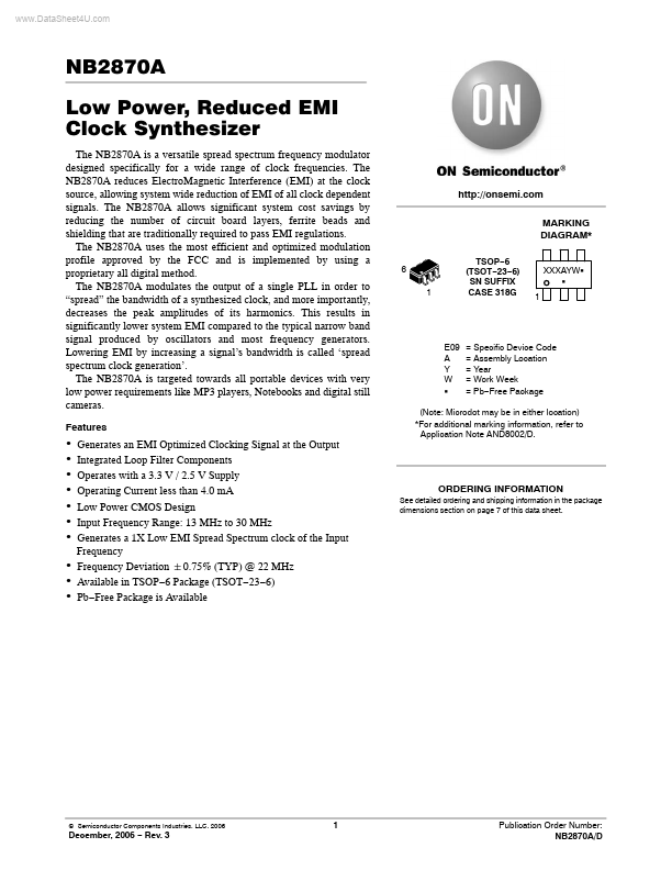
Features http://onsemi. MARKING DIAGRAM-
6 1 TSOP- 6 (TSOT- 23- 6) SN SUFFIX CASE 318G XXXAYWG G 1
E09 A Y W G
= Specific Device Code = Assembly Location = Year = Work Week = Pb- Free Package
- -
- -
- -
- -
- -
Generates an EMI Optimized Clocking Signal at the Output Integrated Loop Filter ponents Operates with a 3.3 V / 2.5 V Supply Operating Current less than 4.0 m A Low Power CMOS Design Input Frequency Range: 13 MHz to 30 MHz Generates a 1X Low EMI Spread Spectrum clock of the Input Frequency Frequency Deviation "0.75% (TYP) @ 22 MHz Available in TSOP- 6 Package (TSOT- 23- 6) Pb- Free Package is Available
(Note: Microdot may be in either location)
- For additional marking information, refer to Application Note AND8002/D.
ORDERING INFORMATION
See detailed ordering and shipping information in the package dimensions section on page 7 of this data sheet.
© Semiconductor ponents Industries, LLC, 2006
December, 2006
- Rev. 3
Publication Order Number: NB2870A/D
XIN/CLKIN XOUT Crystal Oscillator Frequency Divider Feedback Divider REFOUT
Modulation
Phase Detector
Loop Filter
Output Divider Mod OUT
Figure 1. Block Diagram Table 1. KEY SPECIFICATIONS
Description
Supply Voltages Frequency Range Cycle- to- Cycle Jitter Output Duty Cycle Modulation Equation Frequency Deviation VDD = 3.3 V / 2.5 V
Specification
13 MHz < CLKIN < 30 MHz 200 ps (maximum) 45/55% (worst case) FIN/640 "0.75% (TYP) @ 22 MHz
REFOUT XOUT XIN/CLKIN
1 2 3
VSS Mod OUT VDD
5 4
Figure 2. Pin Configuration Table 2. PIN DESCRIPTION
Pin # 1 2 3 4 5 6 Pin Name REFOUT XOUT XIN/CLKIN VDD Mod OUT VSS Type O O I P O P Buffered output of the input frequency. Crystal connection. If using an external reference, this pin must be...