Datasheet4U Logo Datasheet4U.com

NB3H63143G - Programmable Clock Generator

General Description

Figure 2.

Table 1.

Pin No.

Key Features

  • See detailed ordering and shipping information on page 23 of this data sheet.
  • Member of the OmniClock Family of Programmable.
  • Programmable Internal Crystal Load Capacitors Clock Generators.
  • Operating Power Supply: 3.3 V ±10%, 2.5 V ±10%.
  • Programmable Output Drive Current for Single Ended Outputs.
  • I/O Standards.
  • Power Saving Mode through Power Down Pin.
  • Inputs: LVCMOS/LVTTL, Fundamental Mode.
  • Programmable PLL Bypass.

📥 Download Datasheet

Datasheet Details

Part number NB3H63143G
Manufacturer onsemi
File Size 383.83 KB
Description Programmable Clock Generator
Datasheet download datasheet NB3H63143G Datasheet

Full PDF Text Transcription (Reference)

The following content is an automatically extracted verbatim text from the original manufacturer datasheet and is provided for reference purposes only.

View original datasheet text
NB3H63143G 3.3 V / 2.5 V Programmable OmniClock Generator with Single Ended (LVCMOS/LVTTL) and Differential (LVPECL/LVDS/ HCSL/CML) Outputs with Individual Output Enable and Individual VDDO www.onsemi.com 
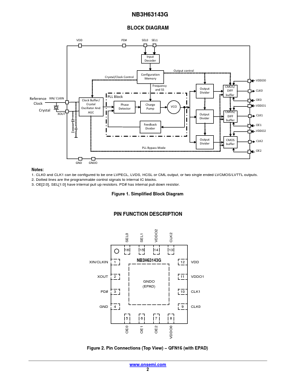
The NB3H63143G, which is a member of the OmniClock family, is a one−time programmable (OTP), low power PLL−based clock generator that supports any output frequency from 8 kHz to 200 MHz. 1 The device accepts fundamental mode parallel resonant crystal or a QFN16 single ended (LVCMOS/LVTTL) reference clock as input. It CASE 485AE generates either three single ended (LVCMOS/LVTTL) outputs, or one single ended output and one differential MARKING DIAGRAM (LVPECL/LVDS/HCSL/CML) output.