NB4L52 Description
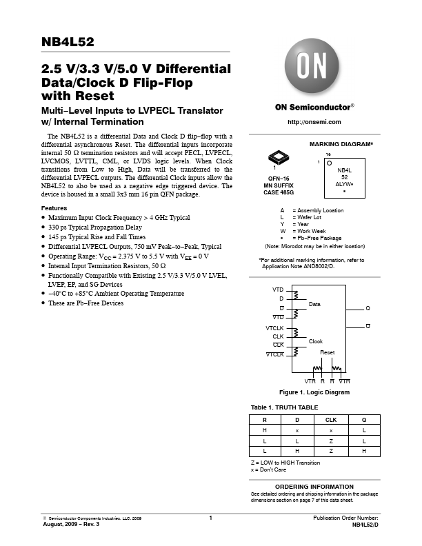
NB4L52 2.5 V/3.3 V/5.0 V Differential Data/Clock D Flip-Flop with Reset Multi−Level Inputs to LVPECL Translator w/ Internal Termination The NB4L52 is a differential Data and Clock D flip−flop with a differential asynchronous Reset. The differential inputs incorporate internal 50 W termination resistors and will accept PECL, LVPECL, LVCMOS, LVTTL, CML, or LVDS logic levels. When Clock transitions from Low to High,...
NB4L52 Key Features
- Maximum Input Clock Frequency > 4 GHz Typical
- 330 ps Typical Propagation Delay
- 145 ps Typical Rise and Fall Times
- Differential LVPECL Outputs, 750 mV Peak-to-Peak, Typical
- Operating Range: VCC = 2.375 V to 5.5 V with VEE = 0 V
- Internal Input Termination Resistors, 50 W
- Functionally patible with Existing 2.5 V/3.3