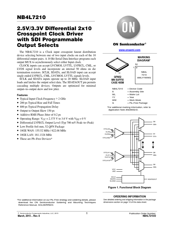
NB4L7210 Description
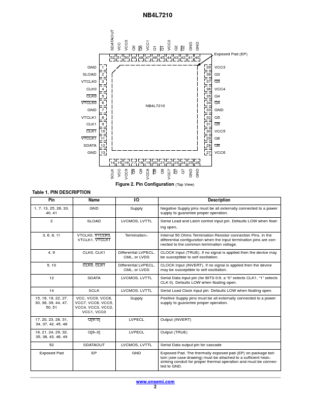
(Top View) Pin Name I/O Description 1, 7, 13, 25, 26, 33, 40, 41 GND Supply Negative Supply pins must be all externally connected to a power supply to guarantee proper operation. 2 SLOAD LVCMOS, LVTTL Serial Load and Latch control input pin. Defaults LOW when float- ing open.
NB4L7210 Key Features
- Typical Input Clock Frequency > 2 GHz
- 200 ps Typical Rise and Fall Times
- 800 ps Typical Propagation Delay
- Output to Output Skew 150 ps
- Additive RMS Phase Jitter of 0.2 ps
- Operating Range: VCC = 2.375 V to 3.6 V with VEE = 0 V
- Differential LVPECL Output Level (Typ 700 mV Peak-to-Peak)
- Low Profile 8x8 mm, 52 QFN Package
- 10GE WAN: 155.52 MHz / 622.08 MHz
- 10GE LAN: 161.1328 MHz