NB6L611 Description
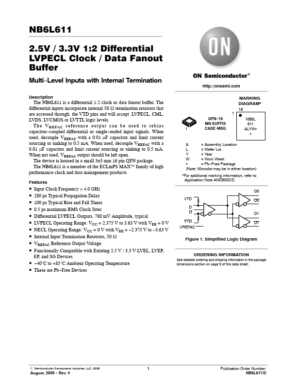
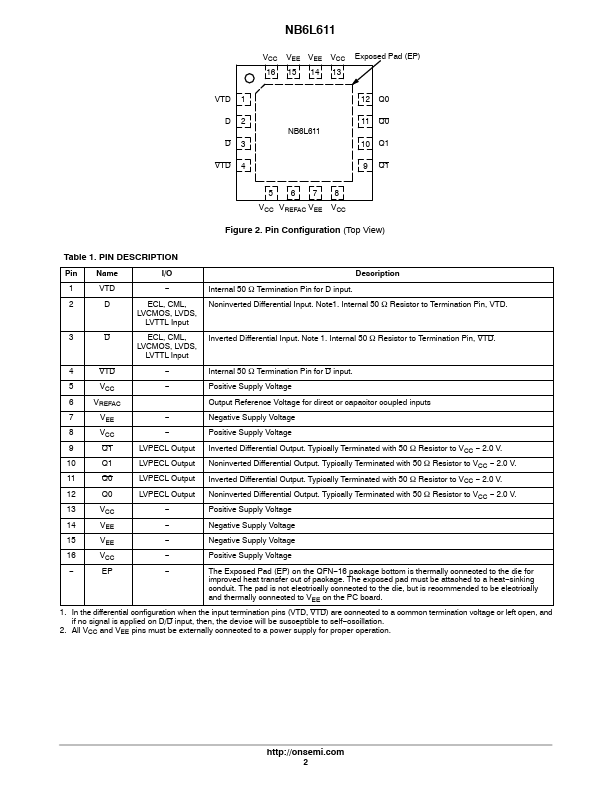
The NB6L611 is a differential 1:2 clock or data fanout buffer. The differential inputs incorporate internal 50 W termination resistors that are accessed through the VTD pins and will accept LVPECL, CML, LVDS, LVCMOS or LVTTL logic levels. The VREFAC reference output can be used to rebias capacitor−coupled differential or single−ended input signals.
NB6L611 Key Features
- Input Clock Frequency > 4.0 GHz
- 280 ps Typical Propagation Delay
- 100 ps Typical Rise and Fall Times
- 0.5 ps maximum RMS Clock Jitter
- Differential LVPECL Outputs, 780 mV Amplitude, typical
- LVPECL Operating Range: VCC = 2.375 V to 3.63 V with VEE = 0 V
- NECL Operating Range: VCC = 0 V with VEE = -2.375 V to -3.63 V
- Internal Input Termination Resistors, 50 W
- VREFAC Reference Output Voltage
- Functionally patible with Existing 2.5 V / 3.3 V LVEL, LVEP