NB6N14S
NB6N14S is Differential Input to LVDS Fanout Buffer/Translator manufactured by onsemi.
3.3 V 1:4 Any Levelt Differential Input to LVDS Fanout Buffer/Translator
The NB6N14S is a differential 1:4 Clock or Data Receiver and will accept Any Levelt differential input signals: LVPECL, CML or LVDS. These signals will be translated to LVDS and four identical copies of Clock or Data will be distributed, operating up to 2.0 GHz or 2.5 Gb/s, respectively. As such, the NB6N14S is ideal for SONET, Gig E, Fiber Channel, Backplane and other Clock or Data distribution applications.
The NB6N14S has a wide input mon mode range from GND + 50 m V to VCC
- 50 m V. bined with the 50 W internal termination resistors at the inputs, the NB6N14S is ideal for translating a variety of differential or single- ended Clock or Data signals to 350 m V typical LVDS output levels.
The NB6N14S is offered in a small 3 mm x 3 mm 16- QFN package. Application notes, models, and support documentation are available at .onsemi..
The NB6N14S is a member of the ECLin PS MAXt family of high performance products. Features
- Maximum Input Clock Frequency > 2.0 GHz
- Maximum Input Data Rate > 2.5 Gb/s
- 1 ps Maximum RMS Clock Jitter
- Typically 10 ps Data Dependent Jitter
- 380 ps Typical Propagation Delay
- 120 ps Typical Rise and Fall Times
- VREF_AC Reference Output
- TIA/EIA
- 644 pliant
- Functionally patible with Existing 3.3 V LVEL, LVEP, EP, and
SG Devices
- These are Pb- Free Devices
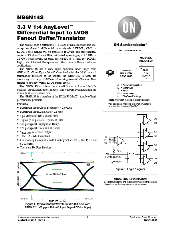
Device DDJ = 10 ps http://onsemi.
MARKING DIAGRAM-
QFN- 16
NB6N
MN SUFFIX
14S
CASE 485G
ALYW G
A = Assembly Location L = Wafer Lot Y = Year W = Work Week G = Pb- Free Package
(Note: Microdot may be in either location)
- For additional marking information, refer to Application Note AND8002/D.
Q0...