NB6N239S
NB6N239S is 3.3 V, 3.0 GHz Any Differential Clock IN to LVDS OUT Clock Divider manufactured by onsemi.
3.3 V, 3.0 GHz Any Differential Clock IN to LVDS OUT ÷1/2/4/8, ÷2/4/8/16 Clock Divider
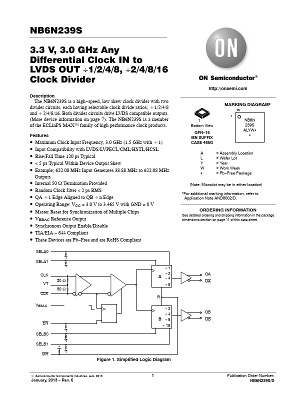
Description The NB6N239S is a high- speed, low skew clock divider with two divider circuits, each having selectable clock divide ratios; B1/2/4/8 and B2/4/8/16. Both divider circuits drive LVDS patible outputs. (More device information on page 7). The NB6N239S is a member of the ECLin PS MAX™ family of high performance clock products.
Features
- Maximum Clock Input Frequency, 3.0 GHz (1.5 GHz with B1)
- Input patibility with LVDS/LVPECL/CML/HSTL/HCSL
- Rise/Fall Time 120 ps Typical
- < 5 ps Typical Within Device Output Skew
- Example; 622.08 MHz Input Generates 38.88 MHz to 622.08 MHz
Outputs
- Internal 50 W Termination Provided
- Random Clock Jitter < 2 ps RMS
- QA B1 Edge Aligned to QB Bn Edge
- Operating Range: VCC = 3.0 V to 3.465 V with GND = 0 V
- Master Reset for Synchronization of Multiple Chips
- VBBAC Reference Output
- Synchronous Output Enable/Disable
- TIA/EIA
- 644 pliant
- These Devices are Pb- Free and are Ro HS pliant
SELA0 SELA1
CLK VT
VBBAC
50 W 50 W
EN SELB0 SELB1
+
B1
B2 B4
B8
B2 B4 B B8 B16
Figure 1. Simplified Logic Diagram...