NB7L72M Description
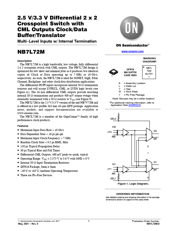
The NB7L72M is a high bandwidth, low voltage, fully differential 2 x 2 crosspoint switch with CML outputs. The NB7L72M design is optimized for low skew and minimal jitter as it produces two identical copies of Clock or Data operating up to 7 GHz or 10 Gb/s, respectively. As such, the NB7L72M is ideal for SONET, GigE, Fiber Channel, Backplane and other clock/data distribution applications.
NB7L72M Key Features
- Maximum Input Data Rate > 10 Gb/s
- Data Dependent Jitter < 10 ps pk-pk
- Maximum Input Clock Frequency > 7 GHz
- Random Clock Jitter < 0.5 ps RMS, Max
- 150 ps Typical Propagation Delay
- 30 ps Typical Rise and Fall Times
- Differential CML Outputs, 400 mV peak-to-peak, typical
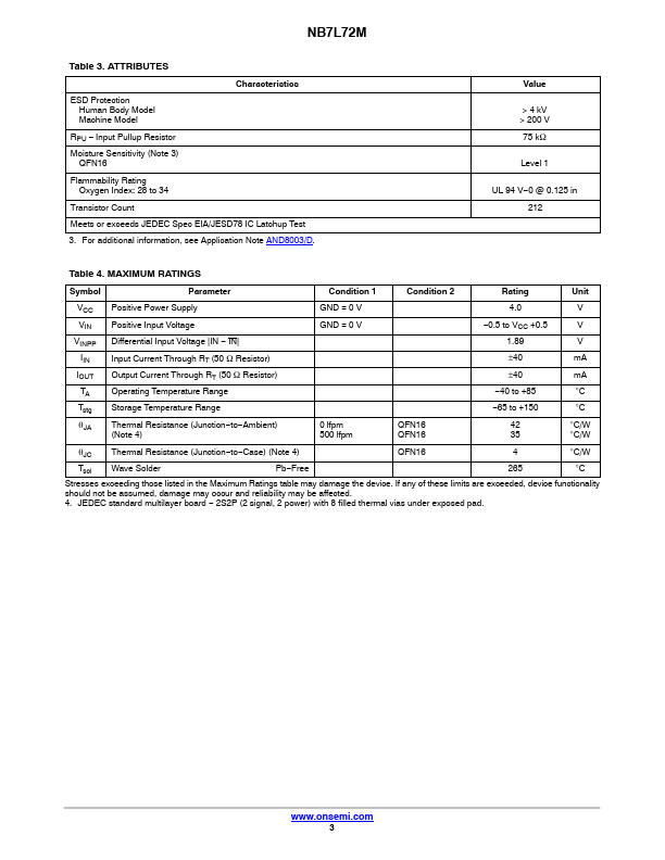
- Operating Range: VCC = 2.375 V to 3.6 V with GND = 0 V
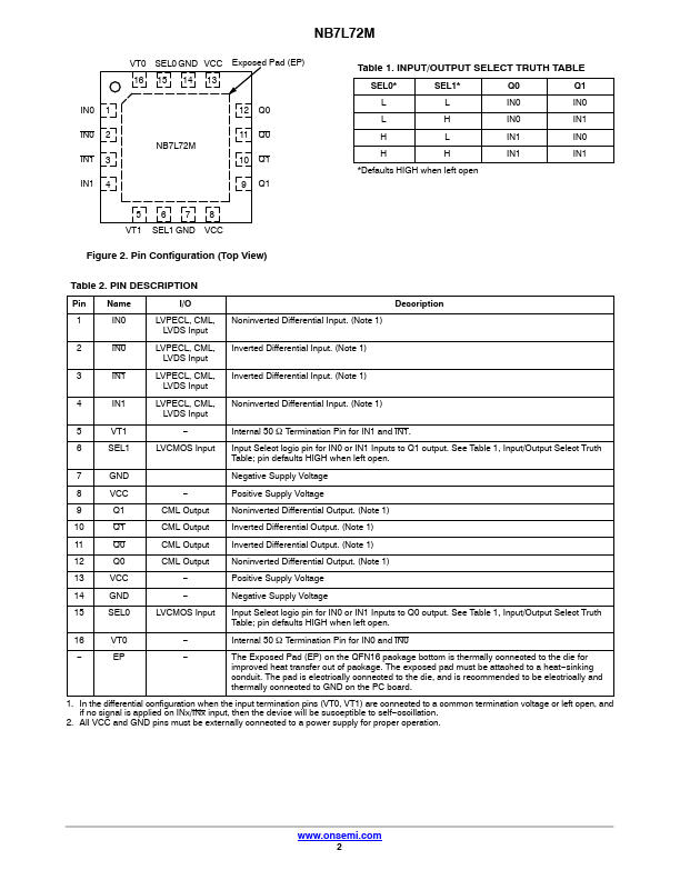
- Internal 50 W Input Termination Resistors
- QFN16 Package, 3mm x 3mm