Datasheet4U Logo Datasheet4U.com

NB7LQ572 - 2.5V / 3.3V Differential 4:1 Mux w/Input Equalizer to 1:2 LVPECL Clock/Data Fanout / Translator

Datasheet Summary

Description

Pin Number 1, 4 5, 8 25, 28 29, 32 2, 6 26, 30 15 18 14, 19 10, 13, 16 17, 20, 23 11, 12 21, 22 9, 24 3 7 27 31 Pin Name IN0, IN0 IN1, IN1 IN2, IN2 IN3, IN3 VT0, VT1 VT2, VT3 SEL0 SEL1 NC VCC Q0, Q0 Q1, Q1 GND VREFAC0 VREFAC1 VREFAC2 VREFAC3 EP LVTTL/LVCMOS Input

Features

  • http://onsemi. com.

📥 Download Datasheet

Datasheet preview – NB7LQ572

Datasheet Details

Part number NB7LQ572
Manufacturer ON Semiconductor
File Size 325.77 KB
Description 2.5V / 3.3V Differential 4:1 Mux w/Input Equalizer to 1:2 LVPECL Clock/Data Fanout / Translator
Datasheet download datasheet NB7LQ572 Datasheet
Additional preview pages of the NB7LQ572 datasheet.
Other Datasheets by ON Semiconductor

Full PDF Text Transcription

Click to expand full text
www.DataSheet4U.com NB7LQ572 2.5V / 3.3V Differential 4:1 Mux w/Input Equalizer to 1:2 LVPECL Clock/Data Fanout / Translator Multi−Level Inputs w/ Internal Termination The NB7LQ572 is a high performance differential 4:1 Clock/Data input multiplexer and a 1:2 LVPECL Clock / Data fanout buffer that operates up to 7 GHz / 11 Gbps respectively with a 2.5 V or 3.3 V power supply. 
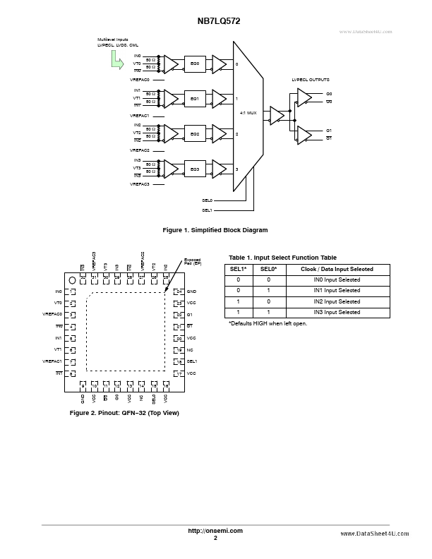
Each INx/INx input pair incorporates a fixed Equalizer Receiver, which when placed in series with a Data path, will enhance the degraded signal transmitted across an FR4 backplane or cable interconnect. For applications that do not require Equalization, consider the NB7L572, which is pin−compatible to the NB7LQ572.
Published: |