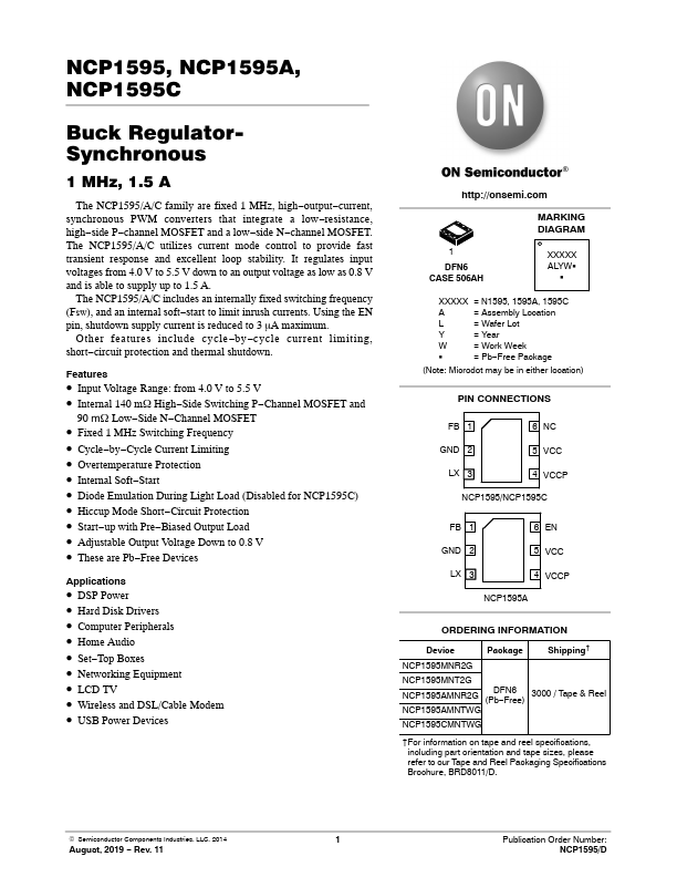
NCP1595A
Description
Feedback input pin of the Error Amplifier.
Key Features
- Input Voltage Range: from 4.0 V to 5.5 V
- Internal 140 mW High-Side Switching P-Channel MOSFET and 90 mW Low-Side N-Channel MOSFET
- Fixed 1 MHz Switching Frequency
- Cycle-by-Cycle Current Limiting
- Overtemperature Protection
- Internal Soft-Start
- Diode Emulation During Light Load (Disabled for NCP1595C)
- Hiccup Mode Short-Circuit Protection
- Start-up with Pre-Biased Output Load
- Adjustable Output Voltage Down to 0.8 V