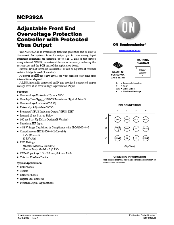
NCP392A
NCP392A is Adjustable Front End Overvoltage Protection Controller manufactured by onsemi.
Adjustable Front End
Overvoltage Protection
Controller with Protected
Vbus Output
The NCP392A is an overvoltage front end protection and be able to disconnect the systems from its output pin in case wrong input operating conditions are detected, up to +28 V. Due to this device using internal NMOS, no external device is necessary, reducing the system cost and the PCB area of the application board.
Internal OVLO threshold is available, or can be adjusted if external resistor bridge is used (A version).
At power up (EN pin = low level), the Vout turns on tstart time after internal timer elapsed.
A LDO, internally connected on IN pin, provided a protected output voltage even if an...