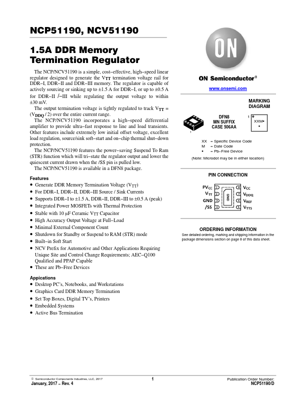
Datasheet4U Logo Datasheet4U.com
onsemi logo

NCP51190

Manufacturer: onsemi

NCP51190 datasheet by onsemi.

NCP51190 datasheet preview

NCP51190 Datasheet Details

Part number NCP51190
Datasheet NCP51190-ONSemiconductor.pdf
File Size 97.99 KB
Manufacturer onsemi
Description 1.5A DDR Memory Termination Regulator
NCP51190 page 2 NCP51190 page 3

NCP51190 Overview

NCP51190 Pin Number Pin Name Pin Function 1 PVCC The PVCC pin provides the rail voltage from where the VTT pin draws load current. There is a limitation between VCC and PVCC. The PVCC voltage must be less or equal to the VCC voltage to ensure the correct output voltage regulation.

NCP51190 Key Features

  • Generate DDR Memory Termination Voltage (VTT)
  • For DDR-I, DDR-II, DDR-III Source / Sink Currents
  • Supports DDR-I to ±1.5 A, DDR-II, DDR-III to ±0.5 A (peak)
  • Integrated Power MOSFETs with Thermal Protection
  • Stable with 10 mF Ceramic VTT Capacitor
  • High Accuracy Output Voltage at Full-Load
  • Minimal External ponent Count
  • Shutdown for Standby or Suspend to RAM (STR) mode
  • Built-in Soft Start
  • NCV Prefix for Automotive and Other
onsemi logo - Manufacturer

More Datasheets from onsemi

View all onsemi datasheets

Part Number Description
NCP51198 1.5A DDR Memory Termination Regulator
NCP51199 Termination Regulator
NCP51100 Low-Side Gate Driver
NCP51105 Low-Side Gate Driver
NCP51145 Termination Regulator
NCP5104 Half Bridge Driver
NCP5106A High and Low Side Driver
NCP5106B High and Low Side Driver
NCP5109A High and Low Side Driver
NCP5109B High and Low Side Driver

NCP51190 Distributor

Datasheet4U Logo
Since 2006. D4U Semicon. About Datasheet4U Contact Us Privacy Policy Purchase of parts