NCP51199
NCP51199 is manufactured by onsemi.
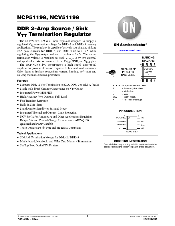
NCP51199, NCV51199
DDR 2-Amp Source / Sink VTT Termination Regulator
The NCP/NCV51199 is a linear regulator designed to supply a regulated VTT termination voltage for DDR- 2 and DDR- 3 memory applications. The regulator is capable of actively sourcing and sinking ±2 A peak currents for DDR- 2, and DDR- 3 up to ±1.5 A while regulating the VTT output voltage to within ±10 mV. The output termination voltage is regulated to track VDDQ / 2 by two external voltage divider resistors connected to the PVCC, GND, and VREF pins.
The NCP/NCV51199 incorporates a high- speed differential amplifier to provide ultra- fast response to line and load transients. Other Features include source/sink current...