NCP5201
NCP5201 is Dual Output DDR Power Controller manufactured by onsemi.
features include soft- start circuitry and undervoltage monitoring of VCC and VSTBY. The IC is packaged in a 5 × 6 QFN- 18.
Features http://onsemi. MARKING DIAGRAM
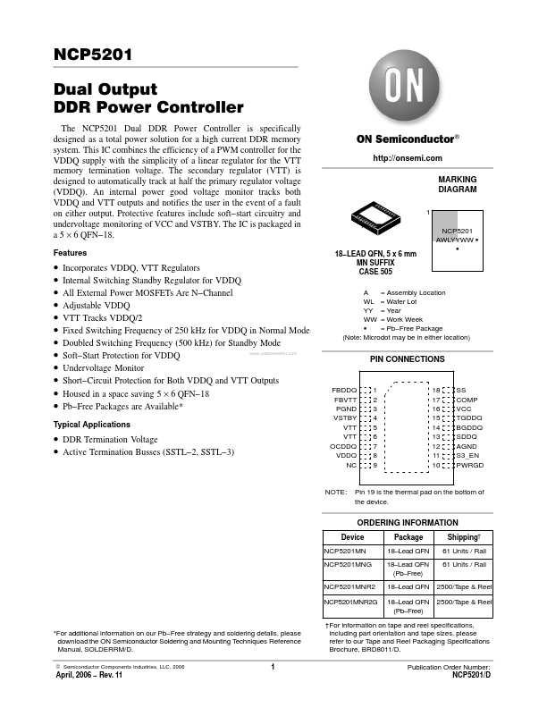
1 1 NCP5201 AWLYYWW G G
- -
- -
- -
- -
- -
- -
Incorporates VDDQ, VTT Regulators Internal Switching Standby Regulator for VDDQ All External Power MOSFETs Are N- Channel Adjustable VDDQ VTT Tracks VDDQ/2 Fixed Switching Frequency of 250 k Hz for VDDQ in Normal Mode Doubled Switching Frequency (500 k Hz) for Standby Mode .. Soft- Start Protection for VDDQ Undervoltage Monitor Short- Circuit Protection for Both VDDQ and VTT Outputs Housed in a space saving 5 × 6 QFN- 18 Pb- Free Packages are Available-
18- LEAD QFN, 5 x 6 mm MN SUFFIX CASE 505
A = Assembly Location WL = Wafer Lot YY = Year WW = Work Week G = Pb- Free Package (Note: Microdot may be in either location)
PIN CONNECTIONS
Typical Applications
- DDR Termination Voltage
- Active Termination Busses (SSTL- 2, SSTL- 3)
FBDDQ FBVTT PGND VSTBY VTT VTT OCDDQ VDDQ NC
1 2 3 4 5 6 7 8 9
18 17 16 15 14 13 12 11 10
SS P VCC TGDDQ BGDDQ SDDQ AGND S3_EN PWRGD
NOTE:
Pin 19 is the thermal pad on the bottom of the device.
ORDERING INFORMATION
Device NCP5201MN NCP5201MNG NCP5201MNR2 NCP5201MNR2G Package 18- Lead QFN 18- Lead QFN (Pb- Free) Shipping† 61 Units / Rail 61 Units / Rail
18- Lead QFN 2500/T ape & Reel 18- Lead QFN 2500/T ape & Reel (Pb- Free)
- For additional information on our Pb- Free strategy and soldering details, please download the ON Semiconductor Soldering and Mounting Techniques Reference Manual, SOLDERRM/D.
© Semiconductor ponents Industries, LLC, 2006
†For information on tape and reel specifications, including part orientation and tape sizes, please refer to our Tape and Reel Packaging Specifications Brochure, BRD8011/D. Publication Order Number: NCP5201/D
April, 2006
- Rev. 11
5V L1 1.0 m H
R2 10 k
R3 10 k
C1 1000 m F
5 VSTBY C4 1.0 m F
12 V C5 1.0 m F
C2 1.0 m F AGND
S3 4 11 S3_EN R6 16 W C10 100 n F R7 1.15 k C11 6.8 n F R12 20 k 8...