NCP5359A
Key Features
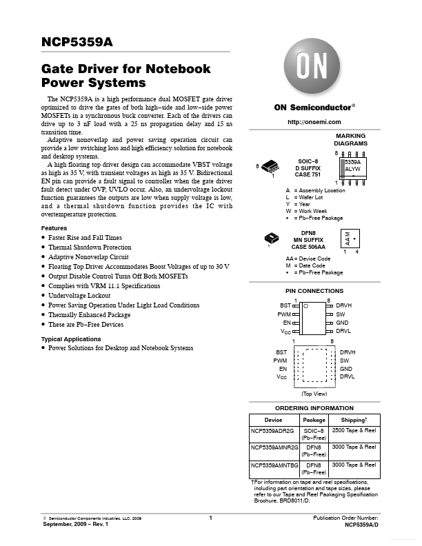
- Faster Rise and Fall Times Thermal Shutdown Protection Adaptive Nonoverlap Circuit Floating Top Driver Acmodates Boost Voltages of up to 30 V Output Disable Control Turns Off Both MOSFETs plies with VRM 11.1 Specifications Undervoltage Lockout Power Saving Operation Under Light Load Conditions Thermally Enhanced Package These are Pb-Free Devices
- Power Solutions for Desktop and Notebook Systems