NCP81071
NCP81071 is Dual 5A High Speed Low-Side MOSFET Drivers manufactured by onsemi.
Dual 5 A High Speed Low-Side MOSFET Drivers with Enable
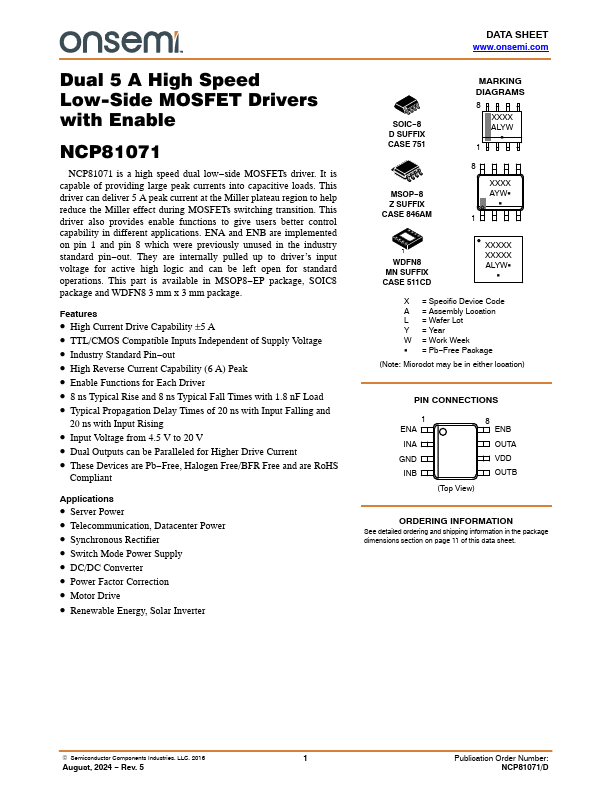
NCP81071 is a high speed dual low- side MOSFETs driver. It is capable of providing large peak currents into capacitive loads. This driver can deliver 5 A peak current at the Miller plateau region to help reduce the Miller effect during MOSFETs switching transition. This driver also provides enable functions to give users better control capability in different applications. ENA and ENB are implemented on pin 1 and pin 8 which were previously unused in the industry standard pin- out. They are internally pulled up to driver’s input voltage for active high logic and can be left open for standard operations. This part is available in MSOP8- EP package, SOIC8 package and WDFN8 3 mm x 3 mm package.
Features
- High Current Drive Capability ±5 A
- TTL/CMOS patible Inputs Independent of Supply Voltage
- Industry Standard Pin- out
- High Reverse Current Capability (6 A) Peak
- Enable Functions for Each Driver
- 8 ns Typical Rise and 8 ns Typical Fall Times with 1.8 n F Load
- Typical Propagation Delay Times of 20 ns with Input Falling and
20 ns with Input Rising
- Input Voltage from 4.5 V to 20 V
- Dual Outputs can be Paralleled for Higher Drive Current
- These Devices are Pb- Free, Halogen Free/BFR Free and are Ro HS pliant
Applications
- Server Power
- Telemunication, Datacenter Power
- Synchronous Rectifier
- Switch Mode Power Supply
- DC/DC Converter
- Power Factor Correction
- Motor Drive
- Renewable Energy, Solar Inverter
DATA SHEET .onsemi.
SOIC- 8 D SUFFIX CASE 751
MSOP- 8 Z SUFFIX CASE 846AM
MARKING DIAGRAMS 8
XXXX ALYW
G 1
XXXX...