NCV51752
Features
- Feature
Options
- VCC UVLO Referenced to GND2
- Built- in Negative Bias between GND2 and VEE Pins
Selectable Negative Bias Levels via Trim
- 3- V to 20- V Input Supply Voltage
- Output Supply Voltage from 6.5 V to 30 V with 6- V and 8- V for
MOSFET, 12- V and 17- V for Si C, Threshold
- 4.5- A Peak Source, 9- A Peak Sink Output Current Capability
- Minimum CMTI of 200 V/ns d V/dt
- Negative 5- V Handling Capability on Input Pins
- Propagation Delay Typical 36 ns with
- 5 ns Max Delay Matching
- AEC- Q100 Qualified for Automotive Application Requirements
- Isolation & Safety
- 3.75 k VRMS Isolation for 1 Minute (per UL1577 Requirements) (Planned)
- CQC Certification per GB4943.1- 2011 (Planned)
- SGS FIMO Certification per IEC 62386- 1 (Planned)
Typical Applications
- On- board Chargers
- x EV DC- DC Converters
- Traction Inverters
- Charging Stations
DATA SHEET .onsemi.
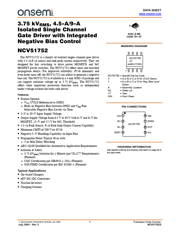
8 1
SOIC- 8 NB CASE 751- 07
MARKING DIAGRAM
NCV51752 XY D AWLYYWW
NCV51752 = Specific Device Code
= A or B or C or...