NSS35200CF8T1G
NSS35200CF8T1G is High Current Surface Mount PNP Silicon Low VCE-SAT Switching Transistor manufactured by onsemi.
es http://onsemi.
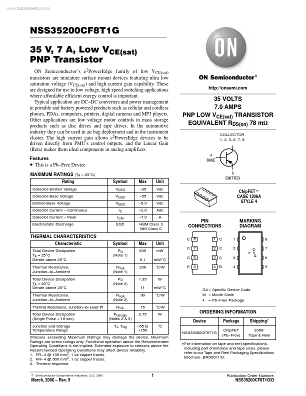
35 VOLTS 7.0 AMPS PNP LOW VCE(sat) TRANSISTOR EQUIVALENT RDS(on) 78 m W
COLLECTOR 1, 2, 3, 6, 7, 8
- This is a Pb- Free Device
MAXIMUM RATINGS (TA = 25°C)
Rating Collector-Emitter Voltage Collector-Base Voltage Emitter-Base Voltage Collector Current
- Continuous Collector Current
- Peak Electrostatic Discharge Symbol VCEO VCBO VEBO IC ICM ESD Max
- 35
- 55
- 5.0
- 2.0
- 7.0 Unit Vdc Vdc Vdc Adc A
4 BASE 5 EMITTER Chip FET] CASE 1206A STYLE 4
HBM Class 3 MM Class C
PIN CONNECTIONS
C 8 1 C 2 C 3 C 4 B 1 2 3 4
MARKING DIAGRAM
8 7 6 5 G4 M G
THERMAL CHARACTERISTICS
Characteristic Total Device Dissipation TA = 25°C Derate above 25°C Thermal Resistance, Junction- to- Ambient Total Device Dissipation TA = 25°C Derate above 25°C Thermal Resistance, Junction- to- Ambient Thermal Resistance, Junction- to- Lead #1 Total Device Dissipation (Single Pulse < 10 sec) Junction and Storage Temperature Range Symbol PD (Note 1) Rq JA (Note 1) PD (Note 2) Rq JA (Note 2) Rq JL PDsingle (Notes 2 & 3) TJ, Tstg Max 635 5.1 200 1.35 11 90 15 2.75
- 55 to +150 Unit m W m W/°C °C/W W m W/°C °C/W °C/W W °C
C 7 C 6 E 5
G4 = Specific Device Code M = Month Code G = Pb- Free Package
ORDERING INFORMATION
Device NSS35200CF8T1G Package Chip FET (Pb- Free) Shipping † 3000/ Tape & Reel
Stresses exceeding Maximum Ratings may damage the device. Maximum Ratings are stress ratings only. Functional operation above the Remended Operating Conditions is not implied. Extended exposure to stresses above the Remended Operating Conditions may affect device reliability. 1. FR- 4 @ 100 mm2, 1 oz copper traces. 2. FR- 4 @ 500 mm2, 1 oz copper traces. 3. Thermal response.
© Semiconductor ponents Industries, LLC, 2006
†For information on tape and reel specifications, including part orientation and tape sizes, please refer to our Tape and Reel Packaging Specifications Brochure, BRD8011/D.
March,...